This thread has been locked.

If you have a related question, please click the "Ask a related question" button in the top right corner. The newly created question will be automatically linked to this question.

TLVM23615: Design Question

Part Number: TLVM23615
Other Parts Discussed in Thread: TPSM365R6, TPSM365R3, LM34926

Dear Team,

1)

is it ok to use TLVM23615 for following conditions: ?

Vin = from 3.6V to 36

Vout = 3.4V  Iout design = 0.3A

Iout max = 0.2A , Iout type = 0.15A

webench.ti.com/.../1111

2) What is the recommended fsw for this condition?

regarding stability and transient response.

3) Would you recommend any other DC/DC for this condition?

Best Regards,

d.

  • Hi,

    Thank you for posting. Let me answer your questions in the same order.

    1) It's a good choice for availability, price and operating temperature range at full load.

    2) To regulate the 3.4V output voltage under the min Vin of 3.4V, the duty cycle should be at least 94.4%.  Because the IC has a min Toff time which limits the max duty cycle, you will need to reduce the switching frequency to not more than 500kHz typical, to leave some margin.

    3). You may take a look at TPSM356R6 which is able to support your load.

    Thanks,

    Youhao

  • Hi Youhao,

    thank you for the replay.

    1) So you don't see any problem using TLVM23615 in our case?

    2) if i setup a webench design with vin from 3.6V to 36V, vout=3.4V and Iout=0.3A -> it sets the fsw = 1MHz

    webench.ti.com/.../SDP.cgi

    is there a n error in webench?

    Please can you provide the equation how to calculate max fsw based on toff_min and duty cycle? How did you get the 500kHz max?

    3) I can't find the part number TPSM356R6 , did you mean TPSM365R6 ? Why would you suggest TPSM365R6 over TLVM23615?

    also i can't create a webench design with TPSM365R3 or TPSM365R6 with Vin from 3.6V to 36V, Vout= 3.4V and Iout=0.3A

    Best Regards,

    d.

  • Hi,

    Sorry for the typo.  It should be TPSM365R6.  I mentioned it just to respond to your question about another part, which is also suitable for your application.

    1) I don't see any problem.

    2). Webench may not consider the worst case conditions. 

    The guaranteed max duty =1 - Toff_min * Fsw = 1 - 85ns * 500kHz = 0.957.  

    3). See the first para. of this reply. Note that the Webench for TPSM365R6 seems presetting the frequency at 1MHz so the required max duty cannot be obtained. However, if you use above calculations, its off time is similar (86ns) so it can produce the required max duty.   Like said, your choice of TLVM23614 is a better one.  Please do not be distracted and stay with TLVM23615.

    Thanks,

    Youhao

  • Hi Youhao,

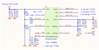
    please can you review our schematic, attached below?

    2)

    2a) I want to set the UVLO so that Von ~ 3.7V and Voff ~ 3.6V ? Is it possible to adjust Ven_hys with external components  ( series resistor) to be closer to 1 ? Do you have a example and formula calculation for TLVM23615?

    2b) i noticed if i set ULVO = 3.6V in Webench ( i assume this is Voff) then Rent=165k, Renb= 100k 

    but if i use this values in eq7 and eg8 i get Von= 3.2595V and Voff=2.324

    so either is WEBENCH not calculating ok or are EQ7 and QE8 not correct, can you please check

    3) in Ds is stated the Cin need to be 4.7uF -> do they mean derated value at max VIn should be 4.7uF ?

    Because the WEBWNCH is only using 4.7uF 0805 50V ( derated only 580nF)

    Best Regards,

    d.

  • Hi,

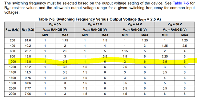
    The schematic basically looks good, but I would suggest you to reserve the connection between RT and VCC to be able to adjust the frequency conveniently by a 0-Ohm resistor. Please note that datasheet suggests the following, although it refers to 2.5A load, but having the flexibility of changing frequency is a good practice. Yes you can still use R26 to program but a 0ohm to VCC may be an easy one.

    Cvcc=4.7uF should work but the datasheet recommends 1uF.

    Answers to your other questions:

    2a)  The hysteresis cannot be adjusted by R10 in your circuit.  It can only work if there is an current source for hysteresis. According to the datasheet, hysteresis seems implemented with a Schmitt comparator, so R10 does not change the hysteresis. Since the build in hysteresis is already 0.353V, you can reduce the hysteresis to 0.1V.

    2b). I think your calculation is correct, and webench has errors. I am checking with our Webench group on this, and will get back to you.

    3). My understanding it the capacitance should be the effective value after the voltage derating. Webench may not correct this but just used a surface value.

    Thanks,

    Youhao

  • Hi Youhao,

    thank you for the feedback.

    1) Regarding 0R from RT to VCC -> fsw=1MHz, but we calculated before if the Vin is 3.6V and Vout =3.4V we can't have fsw more than 500kHz, so i see no point on having this 0R placeholder. ( also i'm very limited with space on the PCB :) )

    2)I used 4.7uf 0402 10V X5R, because when derated for Vcc=3.3V it is ~ 1uF to 1.5uF

    3) where in DS is stated that the hysteresis is implemented with smith trigger and not current source?

    At the end you said " Since the build in hysteresis is already 0.353V, you can reduce the hysteresis to 0.1V. " 

    how can i reduce the hysteresis? is there a way?

    Best Regards,

    d.

  • Hi ,


    Greetings of the day!!

    Please be informed that we have started looking into WEBENCH related query and we will update you as soon as we have solutions for all your queries. 

    Appreciate your patient support.

    Thank you

    Best Regards,
    Sateesh A G

  • Hi Youhao,

    did you have a chance to look at the additional comments and questions?

    Best Regards,

    d.

  • Hi d_zero,

    1) it is just a good practice for having some flexibility which may allow you to use the same PCB for different operating conditions.  You don't have to do it.

    2).That's okay.

    3). It there is current source for hysteresis, it will be given in the ec-table.  Let me copy and paste this device's ec-table regarding UVLO.  To have two thresholds, namely Ven_rise and Ven_hys, it must be a Schmitt triggered comparator.

    Sorry it was a typo:  I was trying to say "you can NOT reduce.."  and wish you can tell from the context.  I am sorry I did not notice it while editing my reply.

    Hope this clarifies.

    By the way, our webench experts are still working on this case, and please allow them some more time.

    Best Regards,

    Youhao

  • Hi Youhao,

    thank you for the feedback.

    Yes of course i will give them some more time Slight smile

    I have some final questions:

    1)

    As our minimal input voltage when the TLVM23615 should regulate is 3.6V to Vout=3.4V, and if i connect EN direct to VIN

    Then if Vin drops below 3.6V we will violate the max duty cycle, what will happen in this case with Vout?

    2)

    I have three options, connect the EN to VIN, use UVLO and Ste Von to 3.6V then Voff = 2.6V or set Voff to 3.6V but then Von= 5V

    What option would you suggest? 

    The 3.6V is the case when 1S LiPo battery is used, and 3.6V is the voltage when we say that the battery is empty, and if our Vin is below 3.6V form our standpoint the TLVM23615 don't need to switch anymore.

    3)

    OR do you maybe have an other solution that could cover this

    Vin=3.6V to 36V

    Vout 3.4V

    Iout_typ = 0.15A

    Iout_max=0.2A

    Iout_design =0.3A for buck

    UVLO_on = UVLO_off = 3.6V  or Von=3.7V Voff=3.6V or something similar

    Best regards,

    d.

  • Hi d_zero,

    We have fixed the reported issue with respect to Webench UVLO and Cin derated capacitor value.
    Currently the fix is in our internal servers and will be available on ti.com by our next Webench release, tentatively by mid of April.
    We will keep you updated on the same.

    For an immediate reference sharing the design report for the reported condition in the link mentioned below.

    /cfs-file/__key/communityserver-discussions-components-files/196/TLVM23615.pdf

    I have moved this post to product expert group for further assistance on above query.

    Thanks and Regards,
    Umayal

  • Hi d_zero,

    Sorry for the delay.  I just found my replies were not sent but remains as draft.  I might have not successfully click Reply.  Let me redo this.

    Hi d_zero,

    Here are answers to your questions.

    1). In this case, Vout would follow and track Vin drop, and  Vout = Vin x Dmax - Rs x Io, where Rs is the equivalent resistance including FET's Rds(ON), inductor DCR, and cable and PCB trace resistances.

    2). I would tie EN to VIN for simplicity, and use PGOOD to tell if the circuit output is in regulation or not. This saves parts, use PGOOD can be used to disable your load circuit, then it would not matter much if the IC is continue to switch under no load.

    3). I searched our module products with integrated FET and magnetics (partially, because TI has lots of products but I am only able to check a few in the time frame), and I haven't found a device support 3.7V on and 3.6V off.   

    To be able to program hysteresis to be 0.1V under 3.7V, you can consider our buck regulator with integrated FETs but employing external magnetics. An example is the LM34926, which has a hysteresis current source to program the hysteresis voltage to be 100mV.

    Best Regards,

    Youhao