This thread has been locked.

If you have a related question, please click the "Ask a related question" button in the top right corner. The newly created question will be automatically linked to this question.

CSD18540Q5B: Power and Thermal Analysis

Part Number: CSD18540Q5B
Other Parts Discussed in Thread: CSD18534Q5A, BQ25756

Hi team,

I have some troubles in my design, regarded to thermal analysis.

I've designed a buck-boost converter (working as boost) with the CSD18540Q5B MOSFET transistor. 

Here, I provide some details of my design:

  • FSW = 250KHz
  • Vin = 20V
  • Vout = 40V
  • Iout = 2A
  • L = 15uHy

Upon conducting the Power Dissipation Analysis, I have obtained the following results:

  • Power @top Mosfet (from buck-boost converter): 1.02W
  • Pbottom @bottom Mosfet (from buck-boost converter): 1.70W

(This analysis comes from: https://www.ti.com/lit/ds/symlink/bq25756.pdf?ts=1709829200271&ref_url=https%253A%252F%252Fwww.ti.com%252Fproduct%252FBQ25756 - 9.2.1.2.8 Power MOSFETs Selection)

Taking into account the RJA and an ambient temperature of 25°C, I estimate:

  • TJ Top = 75.76 °C
  • TJ Bottom = 109.86 °C

However, the thermal measurements conducted with a real PCB board indicate that the MOSFET heats up to 70°C at the case temperature (Based on this measurement, TJ must be greater than the calculated value).

How can I addapt my custom PCB to estimate the case temperature?

Adding another detail to my question is that the estimated loss power is lower than the real.

Thanks

  • Hello Nicolas,

    Thank you for your interest in TI FETs. I have a few questions on how you are estimating the junction temperature rise. Are you using RθJA from the CSD18540Q5B datasheet to calculate ΔTJ? Where are you measuring the case temperature of the FETs? As shown in the datasheet, TI specs RθJA on a standard PCB with 1in² Cu pad and on a minimum pad size. Please see blog at the link below for more information on how TI measures and specifies thermal resistance for our MOSFET packages. As you can see from the blog, RθJA is very dependent on the PCB layout and stackup and the effective RθJA on your PCB may be better (or worse) than the spec in the datasheet. TI can only control RθJC which is measured from junction to the thermal (drain) pad on the bottom of the package. Assuming most of the heat is removed thru the thermal pad on the bottom of the package you can estimate ΔTJ = PD x RθJC. Some heat is removed thru the top of the package (estimated RθJC to the top of the package is about 8°C/W for this FET).

    Other than the simplified calculations using thermal resistance, there are thermal modeling programs to more accurately estimate the junction temperature of the FETs.

    The CSD18540Q5B is our lowest on resistance 60V FET in 5x6mm SON package. The conduction losses in the FETs will be very small while the switching and gate drive losses will be dominant due to the large die size and higher gate charge/capacitance. You could probably use a higher on resistance FET such as the CSD18534Q5A and it may actually reduce the FET losses. The 15μH inductor is going to result in fairly high ripple current which increases the losses in the FETs and inductor.

    https://www.ti.com/document-viewer/lit/html/SSZTB80

    With regards to the losses, are your measured results for the converter or just the FETs? Remember, there are other loss mechanisms (inductor, PCB traces, etc.) that are not taken into account in the calculations from the BQ25756. I hope this helps.

    Best Regards,

    John Wallace

    TI FET Applications

  • Hello John,

    Thanks for your answer. Let me clarify some aspects of my current setup:

    -To know the Junction temperature I'm using the RθJA from the datasheet, I know that it doesn't fit to my current design (I will try to adapt this value to my PCB caractheristics)

    -We are measuring the temperature in the case by two ways. One is with a thermal camera (Flir) and the other is with a thermocouple (fluke) touching the PAD of the transistor. With these measurement we have the same results.

    -To know better my calculous, I leave you attached the python output that takes all the transistor data and make the estimation. I am taking in account the power mosfet loss and too another detected power loss in my circuit.

    power_mosfet_loss.pdf

    Let me know if you detect another loss, I will add it.

    Thanks again!

    Best regards,

    Nicolas

  • Hi Nicolas,

    Thanks for the update. I will review and get back to you next week.

    John

  • Hi Nicolas,

    I'm finally getting a chance to review the pdf document you attached to your previous response. Below is my feedback on the calculations.

    • Gate drive loss formula should be QG x VGS x fsw. You're using VIN instead of VGS. The BQ25756 provides 5V gate drive (V_REGN).
    • Plateau voltage: calculations using 1.9V. Characterization data shows this to be about 3.1V.
    • Thermal resistance: units should be °C/W not W/°C.
    • On resistance positive TC: Rds(on) has a positive temperature coefficient as shown in Figure 8 of the datasheet. This will result in higher conduction loss in the FET at elevated junction temperature.
    • Duty cycle calculation: I use D = 1 - η x (Vin/Vout), where η is the efficiency. I usually assume a value between 90% to 95%.

    I need to spend a little more time reviewing the switching losses. I will get back to you after I have a chance to review.

    Thanks,

    John

  • Hi Nicolas,

    Please take a look at the synchronous boost FET selection tool at the link below. We have similar tools for other topologies and applications as well. The second link is to an app note that has links to all of TI's web-based technical information for our FETs. This tool allows the user to compare up to 3 different TI FET solutions based on 1ku price, power loss or package. The equations tab includes all of the equations to calculate the power loss. As I mentioned in a previous response, the CSD18540Q5B is probably not the best choice for this application. Choosing the lowest on resistance FET does not always result in the lowest overall power loss. Silicon die size is inversely proportional to on resistance for a given FET technology. However, a larger die size equates to larger charge and capacitance which can greatly increase switching loss. Please review and let me know if you have any questions.

    https://www.ti.com/tool/SYNC-BOOST-FET-LOSS-CALC

    https://www.ti.com/lit/an/slvafg3c/slvafg3c.pdf

    Thanks,

    John

  • Hi John,

    Thanks for your help! I will explain some decisions that I took. 

    • For Gate Drive Loss, I used VIN instead of Vgs because the driver datasheet suggest to use this value (regarding that the Vin provides the power)
    • For Plateau Voltage, I cannot understand your value. Can I ask you how to read this from datasheet? Because Table 5.1 gives a Vgs(vth) min typ and max, so that, I used the typical. I'm supossing that you refers to another table, maybe figure 3?
    • For RDS(on) it's true, I will adjust the value regarding to TJ

    I've read your suggestions and documents, It's helpfull to compare similar mosfets.

    After taking in account the Switching Losses and Conduction Losses, we selected the CSD18534Q5A mosfet which reduces both losses.

    Thanks again

    Nicolas

  • Hi Nicolas,

    Thanks for the follow up. Please see comments as follows:

    • OK, I understand. The gate drive loss is in the controller - not the FETs. Since the gate drive voltage is derived from Vin using an internal LDO the calculation is OK.
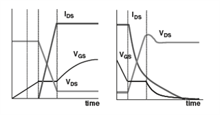
    • TI does not specify the plateau voltage in our FET datasheets. We do measure it on a number of samples during product development. By definition, the plateau voltage is when dVgs/dt is at a minimum. You can estimate the plateau voltage from the gate charge curve on page 1 of the datasheet. There is a region where slope changes and the plateau voltage is roughly in the middle. You can also estimate plateau voltage from the switching waveforms below. Threshold voltage is specified in the datasheet and is the value of VGS where IDS = 250μA and is lower than the plateau voltage.
    • Great.

    As you can see, the lowest Rds(on) FET does not always result in the lowest overall power loss. There is a balance between conduction loss and switching loss.

    Thanks,

    John

  • Great! Thanks for all John!