


Hi,
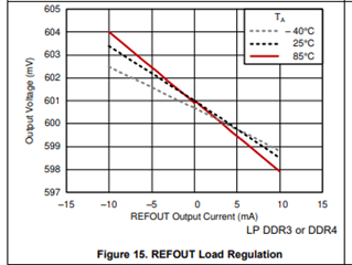
1) Does Output Voltage(mV) in Datasheet P10, "Figure 15. REFOUT Load Regulation" mean VO(3 pin)?
2) If yes, could you provide a graph of "REFOUT Output Current" vs "REFOUT Output Voltage" for DDR4?
Best Regards,
Nishie
Hi,
1) Does Output Voltage(mV) in Datasheet P10, "Figure 15. REFOUT Load Regulation" mean VO(3 pin)?
2) If yes, could you provide a graph of "REFOUT Output Current" vs "REFOUT Output Voltage" for DDR4?
Best Regards,
Nishie
