This thread has been locked.

If you have a related question, please click the "Ask a related question" button in the top right corner. The newly created question will be automatically linked to this question.

UCC28070: Semi-Bridgeless PFC Configuration

Part Number: UCC28070

Hello,

For the Semi bridgeless PFC using UCC28070, can you please help answer this question:

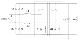
How does the controller identifies if the PFC configuration is interleaved or semi bridgeless. Our understanding is the controller generates output 180 degree out of phase between the 2 FETs which is needed for interleaved PFC but not for Semi bridgeless.

We are referring to this document below but could not find the differentiating factor between the two topologies for controller operation.

UCC28070 Implement Bridgeless Power Factor Correction (PFC) Pre-Regulator Design https://www.ti.com/lit/an/slua517/slua517.pdf 

Thank you, Keith

  • Hello Keith, 

    The UCC28070 controller does not distinguish between the two PFC topologies (or any other topology for that matter).  It merely drives its outputs (basically the GDA and GDB pins) based on the signals present on all the inputs (basically all the other pins). 

    The UCC28070 controller was designed to operate as a 2-phase interleaved PFC and it "thinks" it is still doing that even if reconfigured into a different topology.
    It turns out that the semi-bridgeless PFC configuration is compatible with the operating signals of the UCC28070 and that topology takes advantage of the separate interleaved outputs to drive one of the MOSFETs (say Q1 of Figure 4 of the referenced app-note) during the positive half of the input sine wave and drive the other MOSFET (Q2) during the negative half of the sine.  

    Actually both MOSFETs are being driven at the same time (simultaneously at same switching frequency, but 180 degrees out of phase), but one half of the bridge develops no voltage across the inductor so no current flows in that half line-cycle and all current flows in the other half, and vice versa.  The two phases of the UCC28070 are largely independent of each other although they both receive the same IMO reference and the same VAO error signal.   During a half-line cycle, one phase has no current so that phase's current amp output CAOx is at maximum level (and max PWM duty cycle), but no current can be developed, while the other phase operates normally as a 1-phase boost PFC. This situation reverses to the other phase on the following half-line cycle.  The fact that one of the MOSFETs is switching without current every half-cycle is without significant consequence (although gate-drive loss is incurred).  

    In general, unless specifically designed otherwise, this and most other controllers are not "aware" of the topology or configuration they are being used in, but simply behave as designed according to the signals presented to their inputs.  Different topologies may exploit those behaviors to achieve different design goals, usually to some advantage (such as eliminating a bridge diode loss) at the expense of some other aspect (such as no interleaved currents in both phases). 

    Regards,
    Ulrich

  • Hello,

    Just one thing to confirm. Say during positive half cycle, the device Q1, D1 (during 1-D period), body diode of Q2 and slow Diode Db will be conducting.

    Since we are saying that PWM for Q2 will be at max. duty cycle during entire positive half cycle, the Q2 remains completely ON for that period. So Q2 in fact will see the conduction loss during that period. Is that correct ? I understand that it would be less as it will depend on the current sharing between Q2 and Db. Just to make sure I account for that loss occurring in Q2 & Q1 during each half cycle respectively.

    Thank you, Keith

  • Hello Keith, 

    Yes, you are correct.  In the real world (non-ideal) case, L2 does build up some current (in the negative direction) while Q2 is on during the 1-D intervals of Q1.
    Since Q2 acts like a synchronous rectifier in this situation, it will have very low voltage drop compared to Db, so VDb is applied across L2 for durations (1-D)*Tsw as D changes over the line cycle. 

    Q2 will actually be on only for DMAX*Tsw each switching cycle, but DMAX is typically set around 95% or so, so one could simplify it to 100% and apply a correction factor to account for its body-diode loss during the 1-DMAX interval.  The body-diode would conduct only when L2 pulls current through it when Q2 is off. 

    Meanwhile, L2 current is building by VDb/L2 during the 1-D intervals of Q1, and decaying by -VQ2/L2 during the 1-DMAX intervals of Q2.
    Probably the average 1-D intervals of Q1 can be calculated, but I don't have the math readily available.   

    In a boost converter, 1-D = Vin/Vout, and so 1-D(t) = Vin(t)/Vout.
    At highest lines where Vin_pk is close to Vout, we can approximate 1-D as near 0%, and at Vin = 0V, 1-D = 100%, so (1-D)avg is ~50%.
    At lowest lines where Vin_pk is far from Vout, we can approximate 1-D as >50%, and at Vin = 0V, 1-D = 100%, so (1-D)avg can be 75~80% (for example).

    So in concept, L2 current could build up to I_L2_pk = (VDb/L2)*10ms*80% (for example on 50Hz line).   
    Since half a line cycle (10ms in this example) is a long time, it would seem that L2 current could exceed L1 current.  If so, then diode De would come into play, since the AC source current shouldn't exceed L1 current.  I don't think this would happen, but I don't know for sure, so I don't really know how high L2 current can build up to. 

    Regards,
    Ulrich