This thread has been locked.

If you have a related question, please click the "Ask a related question" button in the top right corner. The newly created question will be automatically linked to this question.

TPS548A28: TPS548A28 burned out due to a current over 4A

Part Number: TPS548A28
Other Parts Discussed in Thread: , TPS54J061

Hello,
 
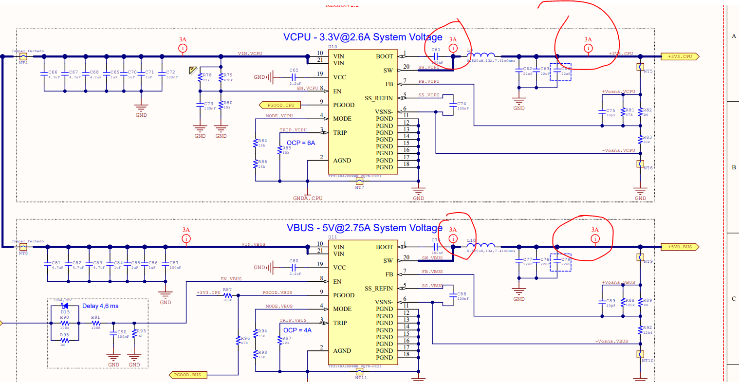
 I designed a source with the TPS548A28 to operate within 3.3V @ 2.6A, with a maximum current of 6A with Vin = 14V and freq = 600kHz.  However, during tests, when demanding a current above 4A, the TPS548A28 shorts the input and output to GND.  After that, I added some capacitors at the input (2x 22uF) and at the output (9x 22uF + 1x 100nF), but the result is still the same.  I also reinforced the GND lines, as my board only has 2 layers in 1/2oz.

image

I took some measurements on the SW output signal to try to understand the reason for this problem.

Figure-3

Figure-2

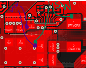
Below are the two layers of this prototype.

image

image

  • Hi Humberto, 
    I am unable to open the pictures.

    Do you have a schematic and layout?

    Can you please attach and send them again?
    Best,

    Ryan

  • Hi Humberto,

    Can you clarify the following questions:

    Are you seeing both devices shorted out at 4.5 A?

    Has this only happened once or multiple times?

    Can you probe the Vin to ensure that the Vin is 14 V?

    Having a high SW ringing could be the issue but based on the waveforms sent they are below the absolute max of 18 V.

    What is the 3A symbol mean on the schematic?

    Best,
    Ryan

  • Hi Rayn,

    Yes, both devices are shorting out.  I have a total of 16 shorted parts, because with each improvement implementation a test was run and caused it to shorted out.
     
     I will measure Vin at higher currents, but for now the measurement carried out only without load and at 2.4A follows.

    Figure_4.pdf
     The 3A symbol is just a technical note for PCB design.

  • Hello Humberto, 

    Ahat is the resolution of the plot you took, we typically need to looks at with 1GHz resolution without BW limit.

    Also where did you measure it, is it at the pin of the device? that where the measurement should be. 

    From your description, the HS FET is shorter, are you able to do ABA test, meaning using a different board to test the failed units 

    Few things that can damage the HS FET: 

    1. Hi VIN (> Abs max of the part)
    2. Hi SW node Voltage ( > SW abs max)
    3. ESD from hot plug, very short but very high spike at the input will cause the device to be damaged
    4. Very high current ( Current Over stress) that can be dues to very high Inductor current  

    Having so many device with this issue, it has to be a systematic issue at system level, please thing within your system, this device has been released for 4 year, with 0 returns.   

    Thanks,

    Tahar

  • Hi Humberto, 

    The datasheet recommends using at least 1 uF capacitor on pin 21 (VIN). It looks like you have a 0.1 uF to VIN on your schematic. Can you try removing it?

    Best,
    Ryan

  • Hi Tahar,
     
     I was actually using an oscilloscope with very low resolution (60MHz).  It took me a while to respond, as I was trying to do this same measurement on a 6GHz device, but it has some problems.  However, when analyzing this on a 500MHz oscilloscope I could already see that my 60MHz oscilloscope was masking significant overshooting.

    So I took measurements using two PCB versions.  One with my original assembly (REV A) and the other with the addition of capacitors in Vin (+2x 22uF) and in Vout (+7x 22uF +1x100nF), in addition to a GND reinforcement with wires (REV B).  In both assemblies (REV A and REV B) I changed the capacitor that was close to pin 21 from 100nF to 1uF as per suggestion.

    VCPU REV A.pdf

    VCPU REV B.pdf

    My measurements were taken at these points with ground spring.

    For a control situation, I'm not using inductive loads, just resistive loads (4R7 resistors in parallel).

    I'm sure this problem is related to my project.  I don't believe it's a characteristic component failure.  However, I would like to find out which part of my project is directly impacting the burning of this component so I can redesign it.

    Thanks,

    1berto.

  • Hi Humberto, 
    Having both the VIN and SW having significant overshoot past their abs max will damage the device. 
    Does the device fail at startup or steady state? Are you able to try using 12 Vin instead and seeing if the device still fails?

    When you turn on the device, do you have the power supply connected first and then turned on, or do you have the power supply on and then hot plugged into the device?

    Best,

    Ryan

  • Já executei esse teste em 10V e realmente obtive mais corrente na saída. Estou conectando a carga após a inicialização.

    Você teria alguma dica para reduzir esse overshooting? Eu poderia resolver isso aplicando um circuito de snubber? A falta de um plano de GND na camada interna poderia ocasionar isso?

  • Hi Humberto, 

    Yes, a snubber can be used to decrease the voltage ringing spikes. 
    I'm not sure if not having an inner layer would cause the VIN to spike that high, but it could lead to having more noise on the other signals on the device. 

    2845.RC Snubber.pdf

    Best,
    Ryan

  • Closing. If any additional assistance is needed, Please post

  • I'm sorry for the late reply.  I was unsuccessful with applying snubber.
     
    Initially I applied 4 different settings without any load current.

    After that, I selected two capacitor options and applied some loads to check the behavior.
     
     with C=1nF:

    with 6.8nF:

    In both cases, the TPS458A continues to burn.
     
     In the meantime I received the TPS548A28EVM development kit and tested it with my load setup.  I was able to prove that it really supports the loads mentioned.

    After that, I used my component configuration (inductor + feedback) and obtained an equally satisfactory result.

    Please note that I am not using any snuber.  Although the voltage peak is high in SW, the TPS548A burns out.

    For my project I ended up switching to the TPS54J061, but I was curious about the reason for the burnout.

  • Hi Humberto, 

    When you used the TPS548A28EVM under your load setup the device was able to deliver the load right?
    And when you switched to the TPS54J061 there was no issues there?
    Best,
    Ryan

  • Yes, using the TPS548A28EVM I had no problems with my loads, but I realized that I would have no control over the current limit in the 3A range.

    My test with the TPS54J061 was only on the EVM and there I could control the current limit as I wanted.  The design of the new PCB is still in the finalization phase and will then be sent for manufacturing.

  • Hi Humberto, 

    Okay, if there are no other issues I will close the thread. 

    Best,
    Ryan