This thread has been locked.

If you have a related question, please click the "Ask a related question" button in the top right corner. The newly created question will be automatically linked to this question.

TPS53355: Why does VREG drop?

Part Number: TPS53355

Hi,

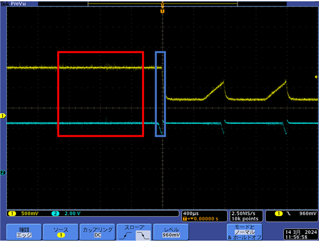
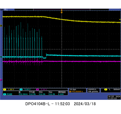
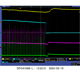
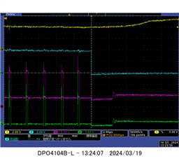
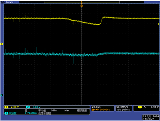
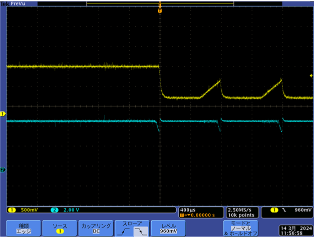
When the load device is Enable, the VREG drops and the VOUT (1.2V) stops. After about 6us, the VOUT/VREG rises and stops again.

This appears to be a VOUT (1.2V) stop because the VREG pin is below the threshold of 3.95V. However, the VDD pins (4.5V to 25V) and EN pins (0.6V) do not fall below the threshold for a moment.

Do you know the cause of this?

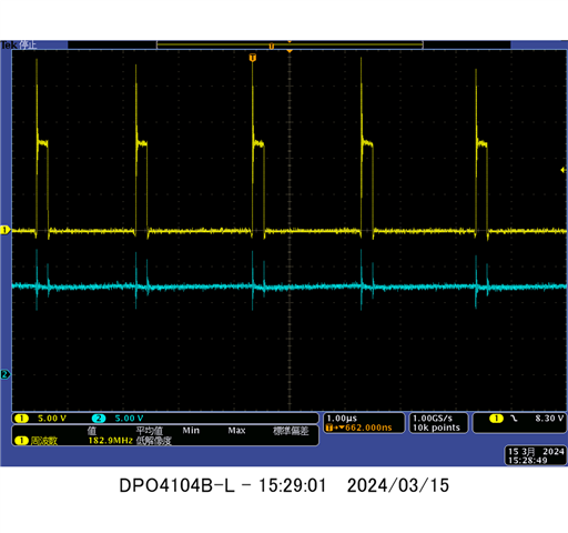
In the following waveform, Ch1 is VOUT and Ch2 is VREG.

A schematic is attached.

6406.Circuit.pdf

Best Regards,

Nishie

  •  

    I don't see anything in the schematic which would likely cause VREG to drop out, though VREG does have an internal current limit which would drop-out if there is excessive loading.

    The fall of VREG at 1.2V in 80μs on 1.0μF bypass capacitance is consist with 15mA of excess loading.

    If you zoom in on the switching node during those last 80μs while VREG is falling, what is the switching frequency?

    It may be possible that something attached to the 1.2V output is turning on and drawing current as it crosses 0.6V, and the converter is significantly increasing switching frequency to continue ramping VOUT, and the gate drive current at the higher switching frequency is exceeding the current limit of the VREG LDO.

    Can you provide an oscilloscope image of the VDD pin voltage, measured right at the pin, during this same time?

  • Hi Peter-san,

    Thank you for your support.

    1)The switch node voltage and VDD terminal voltage in the red frame were measured. Is the measurement point correct? Do you mean the measurement in the blue frame?

    The switching frequency is 500 kHz.

    Ch1 is VOUT、Ch2 is VREG

    Ch1 is VSW、Ch2 is VDD

    2)When the switching frequency is changed from 500kHz to 970kHz, the startup voltage, which was normal at 500kHz, is also dropped. Does the voltage drop increase when the switching frequency is increased?

    Best Regards,

    Nishie

  •  

    1)The switch node voltage and VDD terminal voltage in the red frame were measured. Is the measurement point correct? Do you mean the measurement in the blue frame?

    Sorry for my unclear instructions.  Yes, I meant during the Blue frame when VOUT is dropping.  If you can set VOUT falling at 0.8V as the trigger point and a time scale of 5μs / division, it should give us some insight into what is going on.

    In the graphic you provided of VDD and SW, we can see the loading current is increasing.  If you look closely at the last 2 cycles shown, you can see the slope of the top of the switching node is increasing, dropping more with each cycle.  In addition, the initial voltage on the switching node immediately after the ringing is decreasing.  The drop across the high-side FET is increasing, and the input voltage to the MOSFET may also be decreasing.

    2)When the switching frequency is changed from 500kHz to 970kHz, the startup voltage, which was normal at 500kHz, is also dropped. Does the voltage drop increase when the switching frequency is increased?

    Higher switching frequency will increase the loading on the VREG as turning the MOSFETs on and off more often will require more current.

    The MOSFET drivers essentially need a fixed amount of charge (Q) to turn-on each cycle.  This is called the Gate Charge of the MOSFET, and it's lost (discharged) when we turn the MOSFET off.  The more often we turn the MOSFETs on (higher switching frequency) the more charge per second, which is current, is needed.

  • Hi Peter-san,

    Thank you for your comment.

    The customer measured the switch node voltage(Vsw), VDD and Vout between the blue frames. From this waveform, is it possible for you to answer the cause and solution of this problem?

    1ch: Vout, 2ch: Vsw, 3ch: VDD

    Best Regards,

    Nishie

  •  

    Unfortunately, I am still not seeing anything that would cause VREG to discharge and shut-down, and according to the schematic.  The switching frequency is not rising unexpectedly, and the schematic shows only PGOOD loading on VREG other then the internal gate drives.  While it is showing some ripple, VDD is remaining high and should keep the VREG LDO running.

    While the 3us long SW low period suggests a loading current of 15-18A with the 330nH inductor, we don't see a significant drop on VDD or SW leading up to the VOUT shut-down and VREG drop.

    Since PG is the only other thing loading VREG, would it be possible to get a waveform showing VREG, PG, and VBST during the last few cycles of switching before it shutsdown by triggering on VREG falling ?  I am wondering if R14 might be the wrong resistor value, and a PGOOD trigger is discharging VREG, or if R1 or R2 are the wrong value and 

  • Hi Peter-san,

    Thank you for checking the waveform. I understood that the cause could not be found from the waveform.

    I got a new waveform. Can you tell anything from this waveform?

    Fig.1 1ch: VREG, 2ch: VPGOOD, 3ch: VBST, 4ch: VSW

    Fig.2 1ch: VREG, 2ch: VPGOOD, 3ch: VBST, 4ch: VSW(enlarged view)

    ince PG is the only other thing loading VREG, would it be possible to get a waveform showing VREG, PG, and VBST during the last few cycles of switching before it shutsdown by triggering on VREG falling ?  I am wondering if R14 might be the wrong resistor value, and a PGOOD trigger is discharging VREG, or if R1 or R2 are the wrong value and 

    The last sentence ends with “and ”, is there a continuation? Is it correct to ask the customer to measure the actual resistance values of R1, R2 and R14?

    Best Regards,

    Nishie

  • Nichie,

    The waveforms you provided do not show evidence that the issue is related to R14 and loading on VREG from PGOOD, we see VREG discharging before PGOOD asserts low.

    Your latest waveforms show a Vreg drop of about 1V on 1μF of capacitance over 30μs, an excess loading of about 33mA, which would be consistent with VREG getting turned off.

    You said that EN is not dropping below 0.6V, can you share EN and Vreg?  While a 0.6V input on EN ensures the dissable state, the actual threshold can be somewhat higher in the 1.0-1.2V range.  It is possible EN is dropping down and turning off the VREG LDO, which is then being discharged by the switching of the MOSFETs until it triggers VREG UVLO shutting down and restarting.

  • Hi Peter-san,

    Thank you for checking the waveform. I understand that there is no problem with R14 or PGOOD.

    I also measured the VREG and EN waveforms. Please confirm.

    ■1ch: VREG, 2ch: EN

    For additional information, the customer has identified the following resistance values:

    1) The resistance values of R1 and R2 are 0.9Ohm to 1.2Ohm, respectively.

    2) The resistance was measured between the VBST pin (4pin) and the GNDpin pins on the substrate where the problem occurs. A known-good substrate has a resistance of 40MOhm or more (not measurable by the tester). A problematic substrate has a resistance of 14MOhm to 16.5MOhm. We measured 3 normal substrates and 2 problematic substrates.

    Is this helpful?

    Best Regards,

    Nishie

  • Thank you very much Nishie.

    I also measured the VREG and EN waveforms. Please confirm.

    EN is showing around 4V and never dropping low enough to trigger the turn-off of the VREG, so I don't think that is the issue.

    2) The resistance was measured between the VBST pin (4pin) and the GNDpin pins on the substrate where the problem occurs. A known-good substrate has a resistance of 40MOhm or more (not measurable by the tester). A problematic substrate has a resistance of 14MOhm to 16.5MOhm. We measured 3 normal substrates and 2 problematic substrates.

    14MegOhms should not be discharging BOOT enough to induce the higher loading current required to discharge VREG like we are seeing in these waveforms, but it may be an indication of damage to the BOOT pin that is inducing other issue when the BOOT pin is higher than VIN during high-side switching.

    Can you swap a "known-good" part with a "problematic" part and determine if the issue follows the part or the board?  The part may need to be returned for FA.

    Were the parts purchased from ti.com or through a distributor?

  • Hi Peter-san,

    I am checking with the customer regarding the swap and source of the parts.

    when the BOOT pin is higher than VIN

    Could you tell me the pattern and cause of this phenomenon?

    Best Regards,

    Nishie

  •  

    The BOOT pin normally rises above the VIN pin during operation.  When the high-side FET is on, the SW voltage is pulled to VIN by the internal high-side MOSFET.  The capacitor from SW to BOOT maintains the voltage between the BOOT and SW pin, causing the BOOT pin to rise above VIN.  This allows the driver circuitry for the high-side driver to be referenced to the MOSFETs source, which is connected to SW and continue to power the drivers when SW is pulled up to VIN.

    When the high-side MOSFET is turned off and low-side Turned on, driving SW to GND, the BOOT capacitor is recharged from VREG through an internal diode from VREG to BOOT.

    Normally, the leakage current on BOOT is very low, even when BOOT is 6V higher than VIN, and VREG only needs to supply BOOT with the small amount of charge needed to the MOSFET On and OFF - a few tens of nano-coulombs per switching cycle, but if there is additional leakage on BOOT when it is pulled high, such as might occur from damage to the BOOT devices, VREG would also need to supply that additional current.

    Since VREG is only rated to source 30mA of current, additional loading due to damage to the BOOT circuitry or leakage could cause VREG to discharge.

  • Hi Peter-san,

    Thank you for explaining.

    I will answer the question you asked me before.

    The Swap test is on the way for the customer. Please wait for the results.

    The IC was purchased from Distributor.

    Best Regards,

    Nishie

  •  

    Thank you.  If we find that the part has been damaged, they will need to contact the distributor regarding returning the part or failure analysis.

  •  

    Any progress with an ABA swap of good/bad parts and boards to determine whether the issue is with the board or with the part?

  • Hi Peter-san,

    Sorry for the late reply.

    The customer is in the process of requesting the IC replacement from the board mounting company. Therefore, the result is not known yet. I will contact you when there is progress.

    Best Regards,

    Nishie

  •  

    Thank you for letting me know.  I am setting the post status to "Waiting for Customer" 

  • Hi Peter-san,

    The customer performed a swap test. When a defective IC was mounted on a good board, a defective operation occurred.

    Should this be analyzed? Who should I contact if I want to do an analysis?

    Best Regards,

    Nishie

  •  

    Yes, the device should be analyzed.  Since the device was purchased through a distributor, the customer should contact the distributor per TI's return material policy.

    https://www.ti.com/support-quality/additional-information/customer-returns.html 

  • Hi Peter-san,

    I will proceed with the analysis procedure internally. Thank you for your support.

    Best Regards,

    Nishie

  • Hi Peter-san,

    I tried to analyze it, but my request was not accepted.

    The reason is that the same phenomenon occurred when a good IC was replaced with a defective board based on the results of an ABA swap.

    So I received a pattern layout and a broader circuit diagram from the customer, so could you please check it? I would like to send it via private chat, is that possible?

    Best Regards,

    Nishie

  •  

    Please send me your e-mail address in a private message.

    So that I understand the situation, when the customer swapped parts between a good board and a bad board, both boards starting showing this?

  • E-mail sent.  I am going to close this thread.