Other Parts Discussed in Thread: BQ25790
Hello
I just want to confirm. This is a prototype going to production soon.
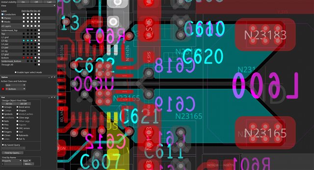
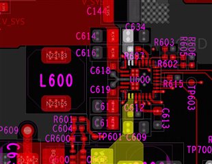
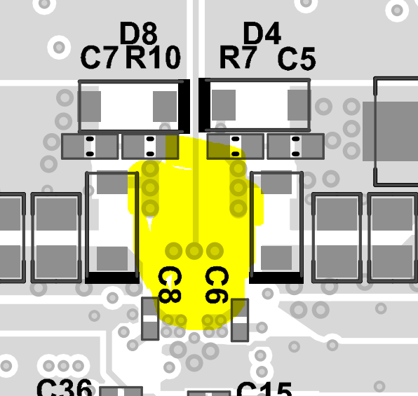
See screendump below. L600 is the inductor, U600 is BQ25792.
U600 and L600 is placed at bottom layer.
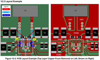
Blue area is the switch node and placed at L3-Sig. Layer up is L2-gnd Solid plane GND. Layer below is L4-pwr this is 3.3V ( processor voltage ) solid layer.
Is this a good layer to place the switch node conductors? Else only alternative is bottom side ( same as component U600 & L600).
Any risk to cause noise at 3.3V plane?
Please let me know your thoughts.
Thank you so much for your help!!