Why is UCC2155x more robust than UCC215xx against VDD supply noise?
This thread has been locked.
If you have a related question, please click the "Ask a related question" button in the top right corner. The newly created question will be automatically linked to this question.
The UCC2155x devices offer a newer, more robust design of the internal ESD cell which better prevents against unintended ESD cell triggering. When noise in the VDD supply triggers the ESD cell, there is a surge in RMS current. Repeated triggers can eventually damage the gate driver. This FAQ will dive into the improvements between the internal ESD cell design of UCC2155x from UCC215xx.
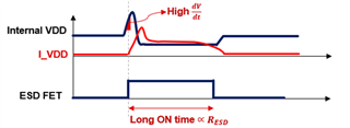
The UCC2155x’s newer ESD cell design allows it to withstand much higher VDD dV/dt values than previous devices. This is due to a fundamental difference in how the ESD cell triggers. With the UCC215xx devices, the internal ESD cell is edge triggered. This means that it is mostly looking at the dV/dt of the VDD waveform. Due to this, high dV/dt noise in the VDD can be seen as an ESD event which triggers the ESD cell to clamp. Looking at Fig. 1, notice how the high dV/dt noise seen on the internal VDD of the UCC215xx device activates the ESD cell.
Figure 1: UCC215xx edge triggered ESD cell event
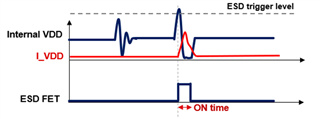
The UCC2155x devices utilize a level triggered ESD cell. A level triggered ESD cell is able to better differentiate noise on the VDD versus an actual ESD event because it looks at the voltage level of the VDD and triggers when it exceeds the ESD trigger voltage level. Notice in Fig. 2 how the first noise transient does not activate the ESD cell despite the high dV/dt. The noise must reach the ESD trigger level to activate the ESD cell. This allows for more robustness against high dV/dt noise transients. A lower overall resistance in the newer ESD cell design also reduces the ON time.
Figure 2: UCC2155x level triggered ESD trigger event
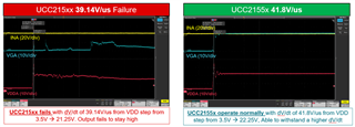
To test this in a bench, data has been taken with a 2-step VDD test. The purpose of this test is to apply a dV/dt on the VDD and monitor the VDD to observe if the ESD cell activates. Looking at Fig. 3, the UCC2155x device is able to withstand a dV/dt of 41.8V/us applied on the VDD. On the other hand, UCC215xx shows failure with a dV/dt of 39.14V/us, showing an unstable VDD supply in the red waveform and an abnormal output in the blue waveform.
Figure 3: 2 step VDD bench data between UCC215xx and UCC2155x. Yellow shows input, blue shows output, and red shows supply rail.