This thread has been locked.

If you have a related question, please click the "Ask a related question" button in the top right corner. The newly created question will be automatically linked to this question.

TPS54360B: How to calculate output capacitance with TPS54360B

Part Number: TPS54360B

ALL HI.

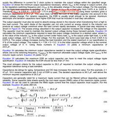
At present, TPS54360B is used for circuit design.As shown in the figure below, how are the parameters in the red box on the figure obtained? How are the values of ΔIOUT and ΔVOUT obtained? All chips are the same?

  • Hello,

    In that particular section, ΔIOUT is your load transient step. For example, if your load transient was a step from 1.5A to 3.5A, then ΔIOUT is 2A (the load change). 

    ΔVOUT is the acceptable change in Vout during the load transient. For example, if the acceptable change is 4% and Vout = 5V, then ΔVOUT = 5 X 0.04 = 0.2V.

    The designer selects their tolerance for ΔIOUT and ΔVOUT. Then, the output capacitance can be calculated for the TPS54360B. 

    ΔVOUT and ΔIOUT are not properties of the IC. Different design requirements will result in different values of output capacitance.

    Best regards,

    Ridge

  •  HI.

    Thank you for your reply.

    What is the basis for stepping this from 1.5A to 3.5A for load transients in the reply? For example, if I use a certain power supply chip how do I determine this step width? What is the basis? What is the basis for the 4% change in Vout? Or is it based on experience?

  • Hello,

    Load transient steps and voltage ripple tolerances are set by the needs of the application, not by the IC. Those values mentioned in the above post are arbitrary examples. When calculating components, a designer would use their selected load transient step and voltage ripple tolerance for their specific application to correctly size the output capacitance. 

    Best regards,

    Ridge