This thread has been locked.

If you have a related question, please click the "Ask a related question" button in the top right corner. The newly created question will be automatically linked to this question.

LM3409HV: LM3409HV Output capacitor recommendation

Part Number: LM3409HV

Hi All,

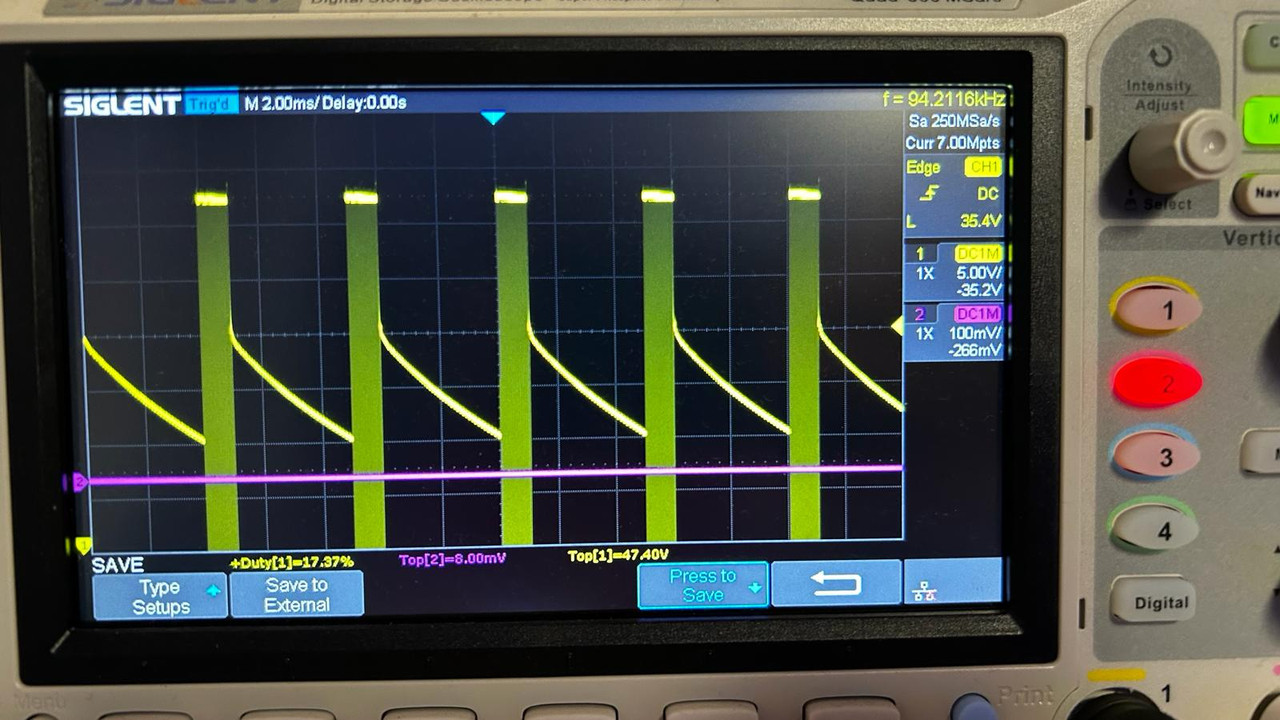
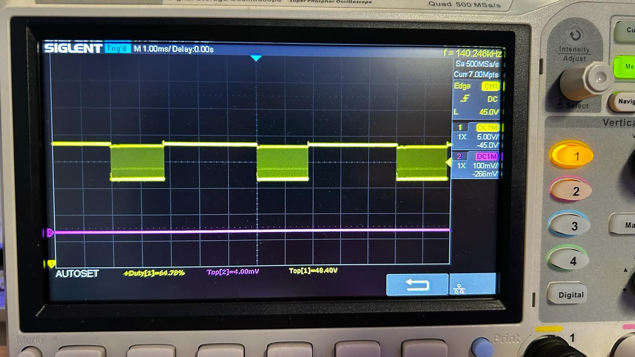
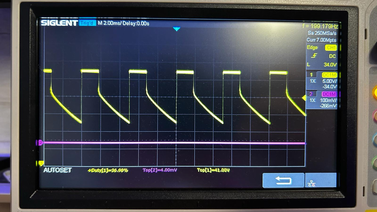
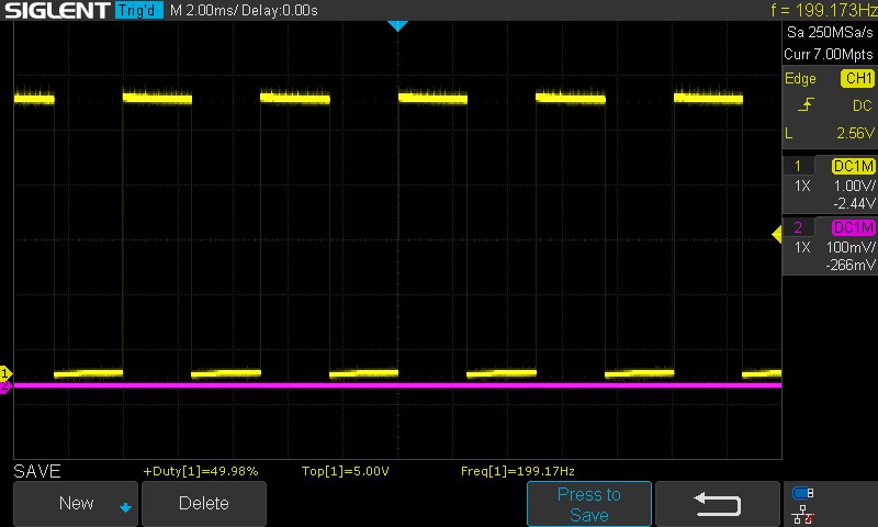
I'm currently building a led driver based on LM3409HV.

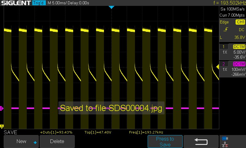
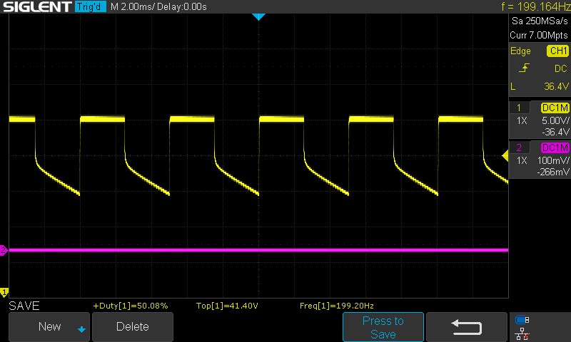
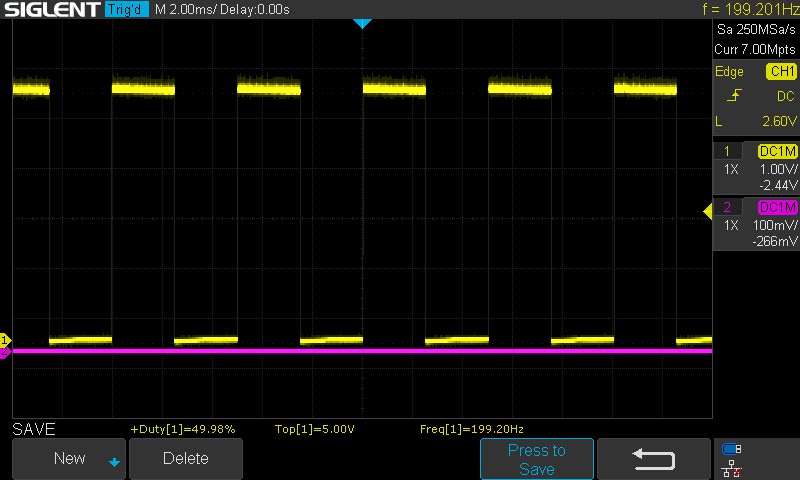
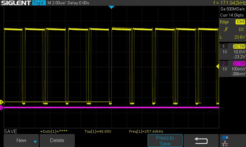
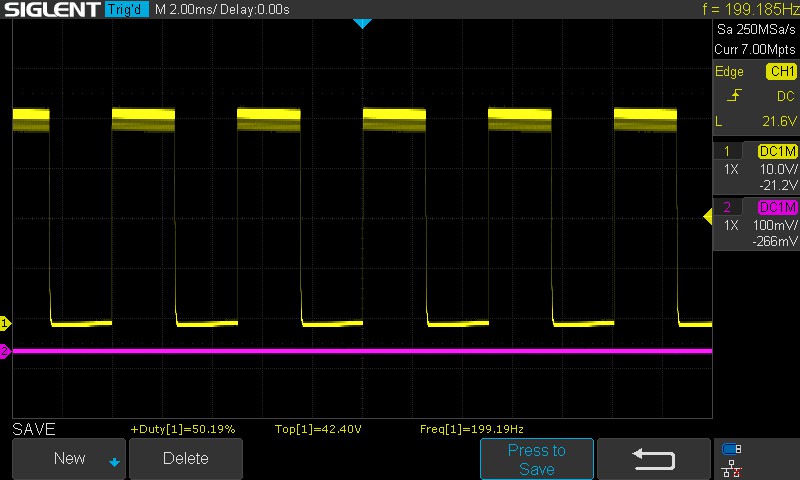
In my test I've seen that using 1uF (for test I'm using cheap electrolytic cap) on output will solve noise problems.

Which cap should I use? I'm looking for an SMD 0805 100V cap.

Thank you very much!

Best regards

Simone

  • You haven't given me any information about the design parameters so it is hard to give you a recommendation.  I would go through the datasheet and use the calculations in the datasheet to figure out component values.

    -fhoude

  • Sorry, I've already calculate the other parts:

    Here I send you a recap:

    Vin: 48V

    Vled: 41,5V

    Iled: 0,75A

    L1: 47uH

    Rsns: 0,28Ohm

    Coff: 470pF

    Roff: 22K

    Ruv1: 6,98K

    Ruv2: 49,9K

    Cin: 2x 2uF 100V

    Q1: ZXMP10A18KTC

    Fsw: 525KHz

    I've done some tests and it seems that 1uF is a good value on the output (very little noise and heat produced).

    I've tryed an SMD capacitor with bad results, switch back to the electrolitic THT and it works just fine. I'm wondering if I have to use some particular type of cap on the output..

    Thank you!

    Simone

  • What do you mean bad results?  Can you share with me waveforms?  Inductor current, SW node, Output voltage, etc?  We use ceramics on the output all the time so I am surprised to hear you having "bad results".  Please define bad results and show them to me.  

    -fhoude

  • I send you some measure,

    Inductor:

    Mosfet gate:

    Output:

    As bad perfomance I have a very "buzzy" noise and much more heat produced. Now I'm using this cap on the output:

    CGA4J3X7S2A105M125AE TDK | Mouser Italia

    If I put an Elna 1uF 100V electrolytic cap on the output the noise is barely udible and the heat produced is much less..

    Tell me if you need more informations. Thank you!

  • Are you saying that you are getting audible noise and that is the "bad result"?  You should be looking at using a different inductor.  That is usually the source of the noise.  Are you sure the capacitor isn't cracked or something?  Try a new or different ceramic capacitor.  What do you mean more heat?  How do you know that?  What is getting hot?  Send me a video is you want.  Send me waveforms too.  I want to make sure it looks like it is operating correctly.

    -fhoude

  • Yes, it is very noisy. I'm using TDK inductor as the example in the datasheet

    SLF12575T-470M2R7-PF TDK | C81468 - LCSC Electronics

    I've also tryed to change the capacitor, even with 2.2uF it produces the same noise.

    The waveforms I sent you looks ok? tell me what else you want to see.

    The mosfet and the diode are getting hot. Qith the electrolytic cap they become barely worm. I haven't measured the temp but the temperature difference can be noticed even with the touch of a finger...

  • I measured the ELNA electrolytic cap and it has an ESR of 3Ohm, while the ceramic is mush lower (around 0.25Ohm) maybe this can be the problem?

  • I forgot to mention that I'm using PWM dimming on the EN pin. I'm sending a 5V 200Hz PWM signal on that pin. 

  • Have you tried a different inductor, something isn't a drum core inductor.  You could try something like the SPM6545VT-470M or  IHLP3232DZER470M51.  

    I want to see the SW node, the inductor current, Output voltage, and EM (PWM) signal.  You should record the temperature of the devices (MOSFET and DIODE) under the two conditions (with and without electrolytic).  If the switching is similar, then I don't understand the difference in losses.  Maybe once I get waveforms I can see what is going on.  

  • Thank you! I don't have other type of inductor but I'll buy the ones you suggest me.

    For SW node you mean the Mos Drain-Diode-Inductor node? Thank you again!

    Also, how do I measure the inductor current? 

  • Hello Simone,

    Yes, that is the correct node.  This should be switching between Vin and ~GND, thus the switching node (SW).  If you lift the inductor to put a loop in series with the inductor to use a current probe, then I recommend lifting the output side of the inductor because you aren't radiating the high voltage switching node into the surrounding circuits.  

  • Thank you again! Right now I don't have a current probe, I'll try to get one as soon as possible. In the meantime I send you some of the other measures:

    WITH ELECTROLYTIC ON THE OUTPUT:

    PWM Singal on the EN pin:

    SW Node:

    Output:

    WITHOUT CAP ON THE OUTPUT:

    PWM Signal on the EN Pin:

    SW Node:

    Output:

    I have to do the temperature measure but the component that heat up the most is the diode (I'm using SS3H10-E3/57T). Inductor and Mosfet are quite warm but not too much (It's A ZXMP10AKTC - maybe I can choose a lower RDS ON mosfet)

  • The waveforms aren't showing up.  You need to use a IR Camera or thermocouple to measure the temperatures in order to see the difference in temp between the normal and electrolytic cap circuits.  Without the inductor current and the SW node it is hard to understand what is going on in a switching converter.  You will NEED a current probe. 

    -fhoude

  • I am going to close this thread and I am assuming you figure it out.