This thread has been locked.

If you have a related question, please click the "Ask a related question" button in the top right corner. The newly created question will be automatically linked to this question.

UC3845: External compensation circuit

Part Number: UC3845
Other Parts Discussed in Thread: TL431, , OPA336, OPA337, LM5025

Hi Team,

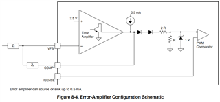
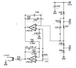
In my design, I need to develop a flyback converter with an adjustable output voltage using an analog signal provided by a DAC. In a previous question that I asked here, I was advised to implement compensation using an external op-amp so that I could utilize this analog reference signal as my voltage source reference voltage. However, I was informed that this external compensation circuit must have an open collector configuration to be directly compatible with the UC's Comp pin. My question pertains to how to create this external compensation circuit with an open collector output. I have searched for relevant documentation, but most of them utilize a TL431 and an optocoupler, which do not support an adjustable reference voltage. Additionally, it's important to note that the voltage source I'm developing should not be isolated. Could you assist me with any documentation or provide a basic schematic of how this external compensation with a variable reference voltage would work?

Thank you.

  • Hi,

    The compensation is in the same way of an amplifier COMP pin not in open collector or open drain.

  • Just to confirm, can I connect the output of an op-amp (OPA336 or OPA337) directly to the Comp pin of the UC3845? Is there no need for an open-collector or drain circuit? I noticed that there is a current source in parallel with the UC's error amplifier output (which I understand is in an open-collector configuration).

    Taking into account the internal current source of the UC, can I design an external compensation circuit with a general-purpose op-amp (OPA337) as shown below?


  • Hi,

    OPA336 337 if their output is not open collector or open drain you cannot connect them directly, as it can damage one of them as you parallel two active comp together.

  • Hi,

    Could you please provide a schematic with a compatible opamp for this application?

  • Hi,

    ok I will provide one within a week.

  • Hi,

    Could you explain how it works? Won't I encounter issues related to the phase of the compensator with this transistor at the output (considering the transistor applies a 180° phase shift)? Given my reference voltage (DAC) ranges from 0 to 5V, would I need to supply the op-amps with a symmetric source (let's say, for instance, +-9V)? Lastly, it seems you took this image from a related document; could you provide it? I genuinely want to comprehend its behavior so I can troubleshoot it independently.

  • Hi,

    This a circuit used in LM5025. The error amplifier is single voltage bias.

    The work is looks the below to achieve negative feedback:

    Vout increase > first amplifier output decrease > second amplifier output increase > transistor collector voltage decrease > COMP voltage lower > duty cycle lower > Vout lower

    if Vout decrease the above change direction becomes opposite.

  • If I want to perform a compensation with just a single pole integrator, one of the op-amps must be configured as a unity gain inverter, right?

  • Hi,

    The 2nd amplifier is in a constant gain (R32/R31) so you can adjust R31 to set up a gain you need. C31 should stay which is a higher frequency path and its associated pole frequency is quite high and it does not form another origin pole. So I suggest you keep the second amplifier as it is until you debugging finds something can be skipped.

  • Isn't the 2nd amplifier gain defined by R32/R31 and R33 is a low pass with C30?

  • Hi,

    Yes R32/R31

  • Okay, thank you for your help!