Dear Support,
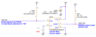
I am using the TLV840MADL29DBV in a design to add a delay to a reset signal generated by an FPGA.
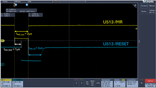
The FPGA drives the /MR input with a 2us low pulse to start asserting the /RESET low (so 2us > tMR_PW).
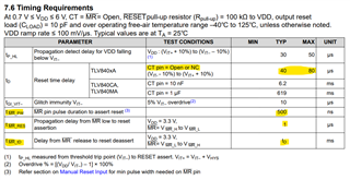
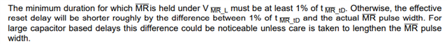
I left the CT pin open so the delay should be 40us typ / 80us max as described on the datasheet p7.
As I understand it, after /MR is logic high again, the delay circuit should keep /RESET low for the 40~80us.
I tested the function, but the /RESET output is only drive low for 2us and release high...
Please find attached the schematic and the scope capture.
Did I missed something? Could you please clarify this point?
Thank you very much for your help.
Kind regards.