This thread has been locked.

If you have a related question, please click the "Ask a related question" button in the top right corner. The newly created question will be automatically linked to this question.

TPS2553D: Device Output failure - Possibly due to Ilim?

Part Number: TPS2553D
Other Parts Discussed in Thread: TPS2553

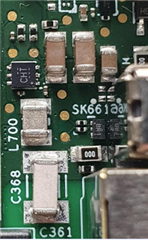
We have a design that is close to volume production and now after a build of 400 units 2 units have failed to output 5V, the output voltage is fed to a USB A type connector shown below.
The design is arranged for auto restart, pin 3 & 4 connected together and current output current limited to ~ 600ma.
When the device fails the following voltages are shown below. the output should be enabled, but seems there is a problem with ILIM.

Any advice would be greatly appreciated.

Pin 1 - Vout - 178mv
Pin 2 - Iim - 0V
Pin 3/4 - Fault/Enable 4.954V
Pin 5 - GND
Pin 6 - Vin - 5.00V
 

  • Hi Richard,

    After some time has passed, are the failing units able to operate normally after a POR? And has the junction temperature been evaluated?

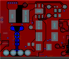
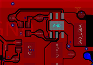
    Everything else looks good schematic-wise, but here is my feedback on the layout:

    1. The layout only shows a handful of GND vias. Thermal vias should be added on the GND copper as much as possible to dissipate heat and provide a low impedance/shorter path for the return current. 
    2. What is the width of the trace connecting Pin1 to the 100k resistor that is also tied to Pin3? Power traces should generally be 10-12 mils.
    3. The trace from Pin5 to the pull down resistor also looks narrow. Narrower traces have increased resistance that attribute to the junction temp. They also do not dissipate heat as easily. 
    4. For future reference, please see the Layout Guidelines and Layout Example sections in the datasheet. 

    BR,

    Seong

  • Hi Seong,

    This layout has 10 layers and the previous picture didn't really show all the vias. The pcb also has more that one ground plane plane that are stitched together for screening as well as dissipation.
    The junction temperature as far as I'm aware has not been elevated at the point of failure. During my testing the device behaved correctly and shut down around 600 mA and then recovered, but in actual fact the device will run at <150 mA if that.

    The device does NOT recover after POR.

    The traces you asked about are 0.1016 mm, I can probably do something to reduce the length of the traces. The power traces are adequate.

    Also, replacing the device fixed my problem, but then fitting the 'none working device' to a known good board exhibited the same issue. No output. So the device is dead with no obvious reason?? Just to clarify, the device was good and working correctly prior to failure.

    regards
    Rich

  • Hi Seong,


    So I've modified the traces to be 10 mils and added more Vias, micro vbisa etc.
    Can you think of why the device died?

  • Hi Richard,

    Can you clarify the full part number of this device? The thread is titled "TPS2553D", but the schematic shows "TPS2553DRVR", which is the TPS2553 that comes in the DRV package. 

    BR,

    Seong

  • Yes this is the TPS2553DRVR, I selected the one nearest in the list of devices.

  • Richard,

    Noted. I will look into this and get back to you shortly.

    BR,

    Seong

  • Hello Richard,

    Apologies for the late response. 

    Could you please let me know how the devices were tested? What was the exact test procedure that led to this fail?

    BR,

    Seong

  • Hi Seong,

    The failure was found in the factory. The test personnel lost comms via USB when connected to a USB mini slave input, used to to upload SW into the units in production. On investigation they found no 5V, replacing the device restored. The slave input, mini usb does not have power and ground on pins 1 and 4, but the shield is connected to gnd.

    These devices failure were found at the final test, so the devices were working at pcb level and fully assembeled.

    regards
    Rich

  • Richard,

    Thank you for clearing this up. So the device was not even overstressed in any manner when it failed.

    Can you share the layout design files? I will send you a friend request so you can send it to me via DM. 

    BR,

    Seong

  • Correct no stress.

    This is the current layout design, the one above show thinkening of tracks and multiple vias added as a precaution.

  • Richard,

    I will DM you so you can send me the original design files of the two boards with failed TPS2553 switches.

    Closing this thread. Please start a new one for any other queries,

    BR,
    Seong