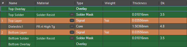
TIDA-050063: What is the preferred PCB Copper thickness (copper OZ) requirements of the physical PCB?
Could you kindly provide me with these technical details or direct me to where I can find this information?
Thank you for your assistance.
TIDA-050063: What is the preferred PCB Copper thickness (copper OZ) requirements of the physical PCB?
Could you kindly provide me with these technical details or direct me to where I can find this information?
Thank you for your assistance.