This thread has been locked.

If you have a related question, please click the "Ask a related question" button in the top right corner. The newly created question will be automatically linked to this question.

TPS6594-Q1: PMIC Shutdown and no I2C communication after applying load

Part Number: TPS6594-Q1

Hi,

We're using the TPS65940400RWERQ1 and are debugging an issue where:

  • PMIC shuts down (nRSTOUT is deasserted) and is no longer accessible over i2c (using EVM and PMIC-GUI 3.0.0) after applying a 2A load on BUCK4.
  • PMIC seems stuck in this state and requires a power cycle to start back up.

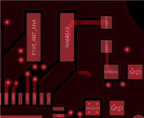
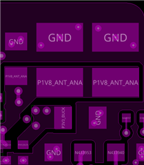
This seems isolated to the BUCK4, loading BUCK3 in the same manner does not cause shutdown. The BUCK4 should be good for 4.5A and we fail already at 2A.

The steps to trigger the behavior is as follows:

  1. Power up board - OK
  2. Check PMIC status over I2C - OK
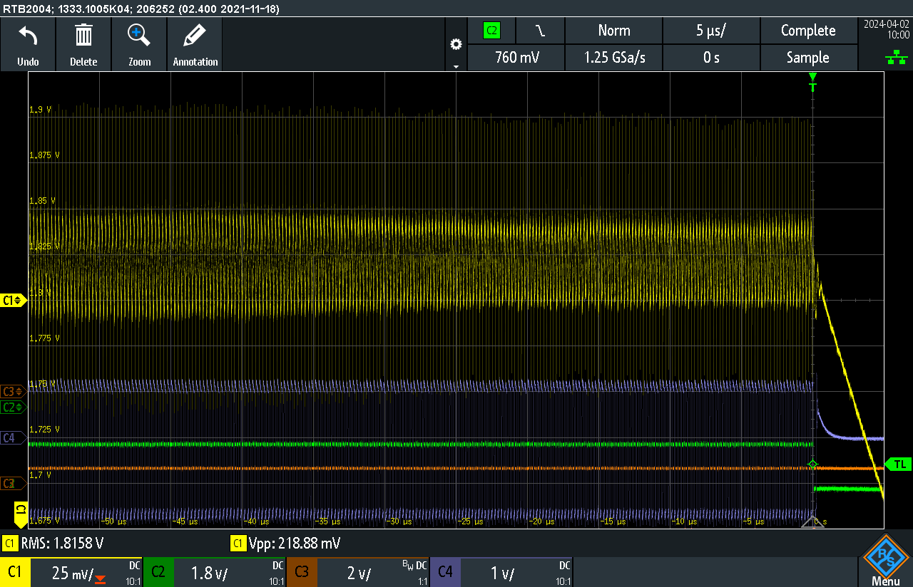
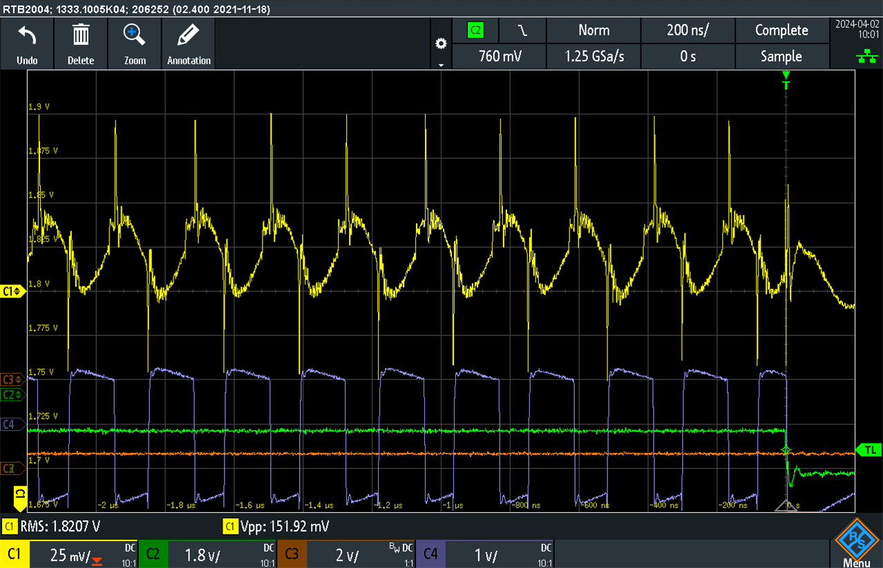
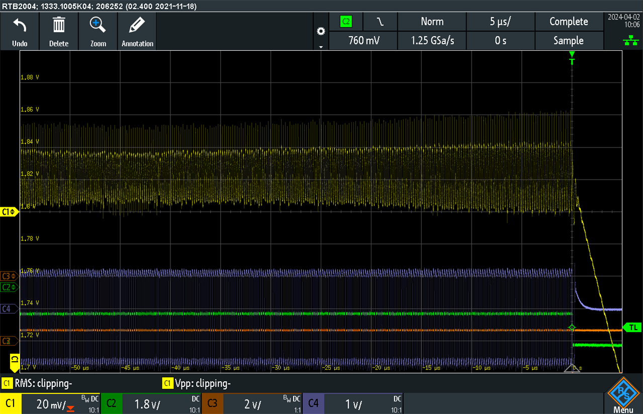
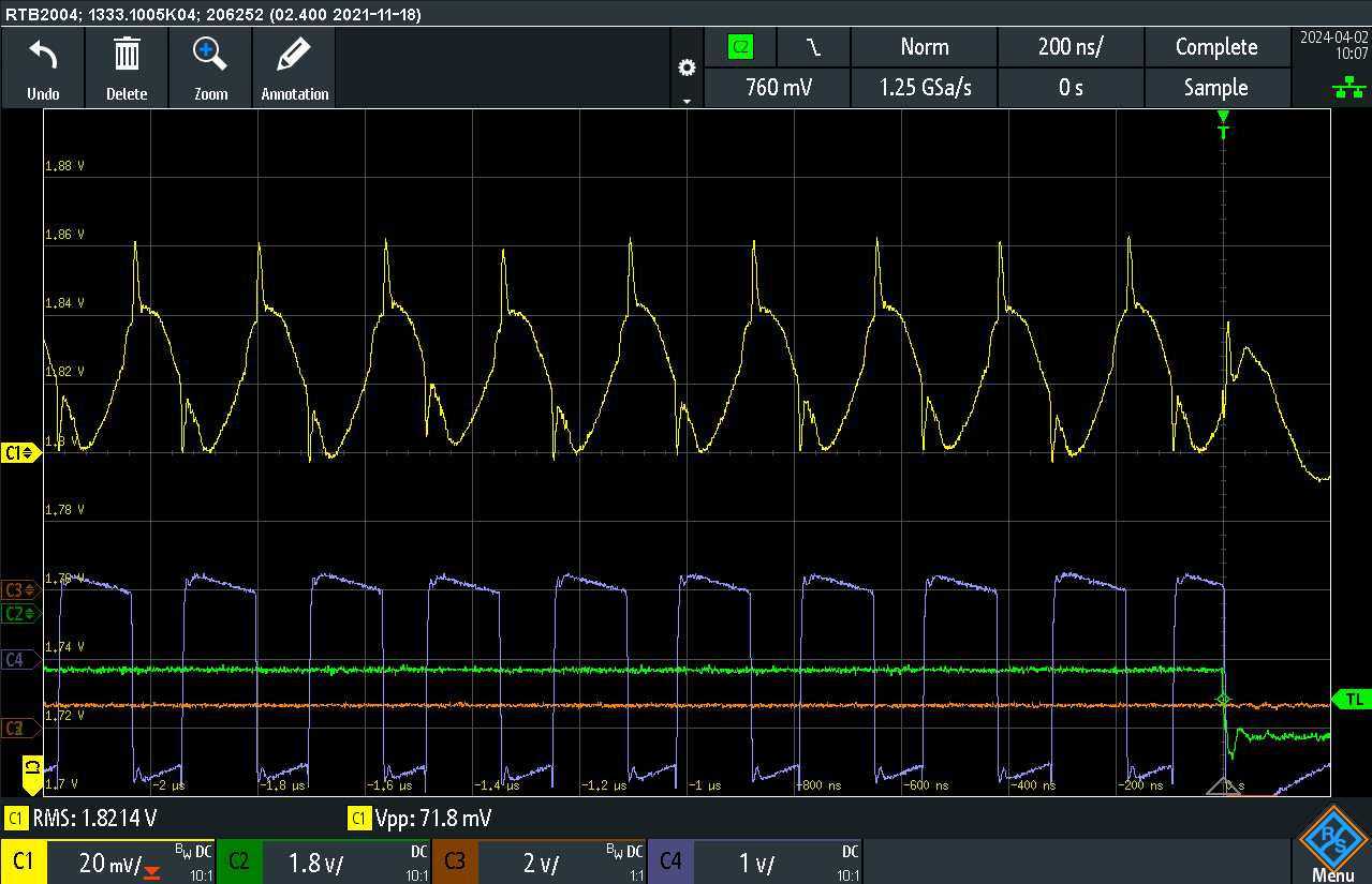
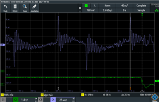
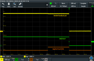
  3. Apply 2 A load using the external DC load - nRSTOUT is deasserted and PMIC is stuck in shutdown (see oscilloscope screen capture)
  4. Check PMIC status over I2C - TI PMIC-GUI can no longer detect the PMIC.

As we are not able to read out the system state after the failure/shutdown has occured, we have no information on what type of failure has occured and how to address the issue. We have access to a BOM-identical design that does not see these issues, as for the boards currently on hand some have this shutdown issue and some do not.

Things we've done to debug the issue so far:

  • Checked incoming supplies - nothing obvious, looks stable when shutdown occurs.
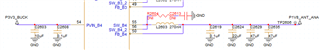
  • Added capacitance and adjusted feedback pin connection slightly - improves noise levels slightly, but shutdown behavior seem similar.
  • Checked temperature dependence using cooling spray - no obvious change
  • Removed all original load from the BUCk4-connected net and connected an adjustable DC load on the outer part of the PDN - able to reproduce the issue reliably.
  • Checked incoming power good signals from external regulators - OK

Have you seen similar issues where the PMIC enters a shutdown state and stops communicating over i2c?

  • Hello Anton,

    We're using the TPS65940400RWERQ1 and are debugging an issue where

    This is the "customer programable" part number for the TPS6594. Are you programming it with a custom NVM? 

    Can you provide the values of the following registers? Registers 0x00A, 0x00B, 0x01B, 0x04A, and 0x08A

    Can you provide scope capture that is zoomed in on the BUCK4 FB while at 2A? Make the vertical scale for the channel 20mV/div and the horizonal scale 5us/div. On the same scope shot, please get the BUCK4 switch node at 1V/div.

    The BUCK4 should be good for 4.5A and we fail already at 2A.

    BUCK4 is rated for 4A DC. But this id dependent on the BUCK4_ILIM setting of NVM. BUCK4_ILIM sets the peak inductor current limit. If it is set to 4.5A, the BUCK control loop will set an internal threshold to prevent the peak current through the inductor from reaching this level. The accuracy of this threshold is +/- 0.55A for the 4.5A setting. So theoretically, it may trigger at 3.95A on some units. A scope shot of the inductor current and switch node would be helpful here.

    Have you seen similar issues where the PMIC enters a shutdown state and stops communicating over i2c?

    If the LDOVINT capacitor is not placed correctly on the PCB, we have seen it cause device shutdown and loss of communication. Please refer to the layout guidelines section of the Data Sheet. 

  • Hi Michael,

    This is the "customer programable" part number for the TPS6594. Are you programming it with a custom NVM? 

    Can you provide the values of the following registers? Registers 0x00A, 0x00B, 0x01B, 0x04A, and 0x08A

    That's correct, we've inherited the NVM configuration from one of our partners and it is also used in at least one more design.

    Here's the register values from NVM and running configuration (after startup):

    Register

    Name

    NVM Value

    Running Value

    0x00A

    BUCK4_CTRL

    0x22

    0x33

    0x00B

    BUCK4_CONF

    0x2B

    0x2B

    0x01B

    BUCK4_PG_WINDOW

    0x12

    0x12

    0x04A

    MASK_BUCK3_4

    0xBB

    0xBB

    0x08A

    FREQ_SEL

    0x1F

    0x1F

    Can you provide scope capture that is zoomed in on the BUCK4 FB while at 2A? Make the vertical scale for the channel 20mV/div and the horizonal scale 5us/div. On the same scope shot, please get the BUCK4 switch node at 1V/div.

    Sure, here's a set of captures with different zoom and BW limit.

    Legend:

    Color

    Probe point

    Yellow (single-ended)

    Feedback

    Blue (diff probe)

    Switching node

    Green

    nRSTOUT

    Orange

    Load

    Full BW:


    20MHz BW on switching node.


    A scope shot of the inductor current and switch node would be helpful here.

    Will try to figure out the best probing approach for this.

    If the LDOVINT capacitor is not placed correctly on the PCB, we have seen it cause device shutdown and loss of communication. Please refer to the layout guidelines section of the Data Sheet. 

    Looks like vi have a via and then the capacitor on the others side of the board here. Do you think that could be the issue. Could try attaching a cap closer to the pin.

    Thanks for your answers so far.

    Best regards,

    Anton

  • Short update here before end of day.

    Tried adding 1 uF close to the VOUT_LDOVINT pin, this seems to increase the possible load to ~2.9A before shutdown. Adding yet another 1 uF (then 2uF in total + existing capacitance), increases possible load to maybe ~3.3-3.4A.

    Still same behavior though: Shutdown and i2c communications loss is permanent until power cycle.

    Additionally, we see that we have quite some ringing at the point of load seemingly caused by the high dv/dt spikes seen in the previous screen captures. Will try to improve decoupling to suppress this behavior.

    Best regards,

    Anton

  • Hello Anton,

    Thank you for al the information, it is very helpful. 

    I believe the noise on BUCK4 is leaking into VOUT_LDOVINT pin and causing a digital reset to occur. Not having proper placement of the cap makes it more susceptible to noise. Hence why adding the extra capacitance helped. 

    Can you provide the piece of your schematic as it relates to BUCK4? Please make sure the FB_B4 line is routed out to the point of load and that there is adequate capacitance after derating. 

  • Hi Michael,

    We suspect something similar (on die EMI or similar ever?) and we do know that the layout isn't ideal around the BUCK4, aiming to fix this to the extent possible in the next board revision that is coming soon.

    Regarding routing the FB line to point of load, it is not possible as there are multiple consumers spread over the board. Expected max load on the B4 rail is somewhere around 2 - 2.5 A. Even so, we are seeing more voltage drop over the plane than expected so we'll beef up the interconnect a bit there.

    There's quite some decoupling involved in several steps, locally to the PMIC there's 116 uF before derating for DC bias, but there's also even more close to the consumers after ferrites and/or pi filters, as this is used as an analog supply. Even after derating, this capacitance should be sufficient as we are using worst case 6.3V rated caps operating at 1.8V. Manufacturer DC bias derating curves indicate little loss of capacitance.

    Again, in the current measurements where we get good reproducibility of the issue, we have reduced the testcase to attaching an electronic DC load at the most remote point but before any additional filtering.

    Here's an overview of how the BUCK4 rail is distributed, dark orange colored plane is the BUCK4 output.

    The feedback is currently positioned next to the inductor, in the same node where it connects to decoupling and bulk capacitors on the other side of the board. (Feedback pin is the centermost pin, you can see the vias going though as circles in the plane)

    We have seen that the noise on the rail can be reduced to some extent by adding capacitance on the PMIC side to calm the FB node a bit, but with diminishing returns and no change in the "permanent" shutdown behavior.

    Finally, here's the schematic part relating to BUCK4:

    Are there any modifications we could try to narrow down the root cause?

    Best regards,

    Anton

  • The feedback is currently positioned next to the inductor, in the same node where it connects to decoupling and bulk capacitors on the other side of the board. (Feedback pin is the centermost pin, you can see the vias going though as circles in the plane)

    This is the source of the high noise on BUCK4 which causes problems for the LDOVINT. 

    Your diagram highlights 4 POL for BUCK4. If you know that one of them will have the largest load pull, I recommend routing to that POL. 

    Also a FB line should be thin and preferably shielded to prevent noise from getting in.