This thread has been locked.

If you have a related question, please click the "Ask a related question" button in the top right corner. The newly created question will be automatically linked to this question.

LM5156: Circuit to generate 90V using LM5156

Part Number: LM5156

Hello Experts,

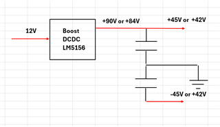
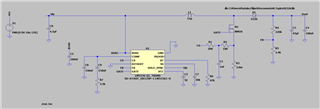
I create the desing to generate 90V using LM5156.
I use the same design from the WEBENCH

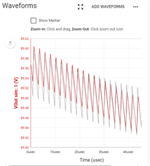
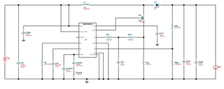
I took this design and simulated in the LTSpice.

For some reason the Vout is 22V for LTSpice, whereas in the WEBENCH is 89V.

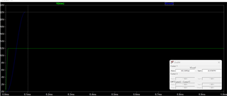
Why is it happening? Do you know what is the issue?

Thank you,
Best,
Filipe S.

  • Hi Filipe,

    Thanks for using the e2e forum.

    If I understand your design correctly, you want to boost a 12V voltage up to 90V, correct?
    With a boost ratio like this, you are very close to the max duty cycle capabilities of the LM5156 device.
    If the device is capable of maintaining the required duty cycle also depends on switching frequency.

    In LTSpice, can you simulate the SS, FB, COMP and CS votlage as well?
    This will show if the device falls into a protection mode like OCP and therefore cannot reach a higher output voltage.

    The softstart cap (C7) has a value of 56kF. Is this a mistake?

    Best regards,
    Niklas

  • Hi Niklas,

    Yes, I would like to convert 12V to 90V or 84V.
    After creating 90V, I would like to spplit in +45V and -45V to supply 16ch of Op Amps.
    See the picture before.


    With a boost ratio like this, you are very close to the max duty cycle capabilities of the LM5156 device.
    If the device is capable of maintaining the required duty cycle also depends on switching frequency.
    →The WEBENCH is showing the possibility. Is not possible to do it as shown in webench?

    In LTSpice, can you simulate the SS, FB, COMP and CS votlage as well?
    This will show if the device falls into a protection mode like OCP and therefore cannot reach a higher output voltage.

    Do you know how can I achieve this voltage?

    Best Regards,
    Filipe Satake

  • P.S.:And about the C7, it was a mistake. I have correct to C7=56nF. And the result is the same.

  • Hi Filipe,

    Thanks for the update.
    The block diagram sent might be slightly misleading, as the Boost output voltage cannot be split into half by capacitors alone.
    If a positive and negative output voltage is required, you might consider a flyback topology with LM5156, which can directly create a positive and negative output rail.

    Regarding the boost ratio,
    In theory it should be possible to achieve this boost ration, just as Webench suggested.
    My point is that this operation is very close to the maximum limit the device can provide, so small variances and efficiency losses can lead to failures.

    E.g. if the device runs with lowest switching frequency of 100kHz, a worst case max duty cycle of 90% is possible, which would be sufficient for this design.
    At 2.2MHz fsw, this would not be possible.

    The simulated signals I requested are meant to find the source why the device cannot achieve the output voltage.
    You can also measure the SW note signal in the simulation to check if the device is running close to the maximum duty cycle. 

    Unfortunately, I have no experience with LTSpice simulations (we only work with PSpice), so I cannot help with the simulation itself.

    Best regards,
    Niklas

  • Hi Niklas,

    Thank you for your explanation.
    I will try to use the Flayback topology to achieve this value of output.

    I tried to see the SW frequency in thhe simulation, but I didn`t get any realistic value.
    The SW frequency you mean is the output of GATE pin, right?

    Do you think if I use 2 stages will be better?

    Best Regards,
    Filipe Satake.

  • Hi Filipe,

    Yes, to measure the duty cycle, you can either take the GATE signal, or put a probe on the note connecting L1, M1 and D1, which is called the switch node.
    Before switching to two stage, I would try to find out what is causing the error in the current design.
    Just as Webench suggested, this design should be feasible if the modification is done correctly.

    Best regards,
    Niklas

  • Hi Niklas,

    Thank you so much.
    I will try to do here, and I will let you know if I get some news results.

    Best regadrds,
    Filipe Satake