This thread has been locked.

If you have a related question, please click the "Ask a related question" button in the top right corner. The newly created question will be automatically linked to this question.

BQ25750EVM: Charger and BATFET not working, if additional load is present to VSYS

Part Number: BQ25750EVM
Other Parts Discussed in Thread: BQ25750, BQ25756, , BQSTUDIO

Hi, TI-team,

Background:

We want to use the BQ25750 as battery charger for 4S1P or 5S1P li-ion. Furthermore we want to use the power path capability. Especially we want to have the ability to switch between normal battery use (BATFET) and auto-reverse mode.
We decided to buy a BQ25750EVM board. Since this is out of stock until July, we bought a BQ25756 board and changed all the relevant components:

BQ25756 changed to BQ25750RRVR (BQ25750EVM =  BQ25750RRVT)

At VSYS connection:
C77, 1µF assembled.
C63, 100nF assembled.
C151, 1nF assembled.

At Pin 32, SYS:
C200, 100nF assembled.
R100, 0 ohms assembled.
R101, 0 ohms removed.

At the FETs for VIN:
R12, 0 ohms assembled.
D1, SZBZX84C15LT3G assembled.
Q5 and Q6, AONS66917 assembled.

R1000 and R1001, 0 ohms removed.

At the BAT_FET:
Q7 and Q8, AONS66917 assembled.
R9, 0 ohms assembled.
R1004 and R1005, 0 ohms removed.

J2 (VSYS) assembled.

Furthermore, since the current range is considerably high we have changed the shunts R2 and R24 both to 20mR (knowing that the values given in bqStudio 1.3.124 have changed accordingly).
File = Charger_1_00-bq25750.bqz

Problem (in test 21V power supply, 4S1P battery, Icharge = 0.5A, optionally: load 15R at VSYS):
If a (resistive) load is connected to VSYS (we assume, this is the intended output for using power path, see also below), then auto-reverse is working when switching between charge/discharge, but with auto-reverse off (i.e. BATFET on) neither charging works nor discharge, the IC falls into a periodically loop trying to switch BATFET. Without any load, BATFET mode works. Connecting the load after switching works also.

We have double-checked the modifications and changed the BATFETs. The behavior persists. Also changing to 'ideal diode' mode gives the same result. The same is true for playing with current limits. Shorting shunts has no effect.

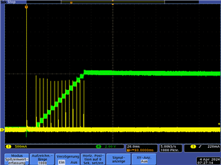
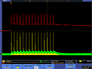
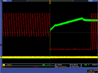
When monitoring the BATFET drive signal, one can see a number of short pulses, increasing VSYS over roughly 40 ms with no load (which we feel a long time). If a load is attached when toggling between charge/discharge, again pulses come, but without fully activating VSYS.
Also strange: When trying to charge, the STATUS output gives "power not good" periodically. It looks like the IC resets internally. However, register content remains present.

What are we doing wrong in BATFET mode?

Questions regarding datasheet:

There is not much info in the datasheet telling anything about the BATFET or ACFET drive signal besides drive voltage and current . So we have no idea, if the gate drive pulsing is normal or not.
Furthermore, we are confused about figures 9.13 and 9.14 'Reverse mode power up and down with load'. Ch2 is labeled with VAC and VAC comes and goes in the diagrams. But ACFET is off in this case, datasheet:

"8.3.6 Reverse Mode Power Direction
The device supports buck-boost reverse power direction to deliver power from the battery to the system when the adapter is not present. During this mode of operation, the ACFET and BATFET both remain off. ..."

So, how can there be an output voltage at VAC? And what is the idea of reverse mode input current regulation (IAC_REV)?

  • Hi Guenter,

    I just want to make sure I understand your problem correctly before I proceed to work on it.

    So assume resistive load is connected and auto reverse is turned ON and no Vin, then no problem.

    If auto reverse is OFF which should be the default setting and no Vin, BATFET does not work ? Same conditon but if there is no load, BATFET works fine and if load is connected after system is already working, it also works fine ?

    Regarding the datasheet, ACFET and BATFET are indeed both OFF. There is a typo in both graphs. The label that says VAC is actually VSYS. Thanks for pointing out the mistake.

    Regarding the IAC_REV, the reverse mode also offers output current regulation via the RAC_SNS resistor. This parameter is controlled by the IAC_REV register bits.

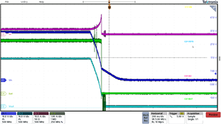
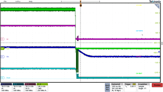
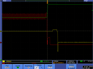
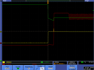
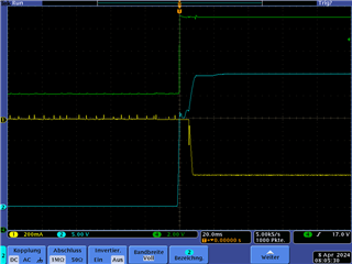
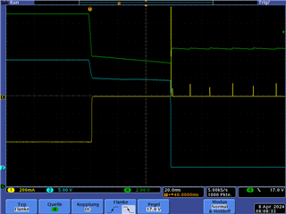
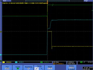
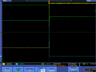
  • Please see below our power path transfer waveforms for no load.

    Please see below for 0.5A load.

  • One more thing that comes to mind is that did you just turn auto reverse off or did you turn off EN_REV as well because it is possible that although auto reverse is off, EN_REV must also be turned off and that may be the issue here.

  • The problem also persists if I do not use I²C at all:

    - Load is connected to VSYS, nothing else (no VAC)
    - Connect battery to VBAT (J3)

    => no VSYS

    Related measurements:

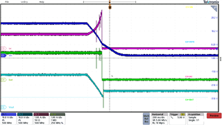
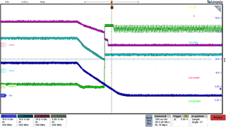
    Ch1 = current sense battery
    Ch4 = VSYS
    M = BAT_DRV - BAT_SRC = VGS BATFET

      
    no load (first current pulse comes from charging caps at VBAT)                                    with load

    VREGN remains 0V, since no charging is active

    The BATFETs are AONS66917 (like EVM schematic). On my opinion, VGS of BATFET is not high enough to reach low RDSon (Gate Threshold Voltage = 1.7 to 2.8 V).
    For the same reason the 'no load' voltage rises considerably slowly. 

    Is the VGS drive signal as expected?

  • Can you please confirm that EN_AUTO_REV and EN_REV are both off ?

    We suggest using AONS6276 for the ACFET and BATFET.

  • Yes, both EN_AUTO_REV and EN_REV are 0 (read back.
    You mean AON6276 (I didn't find AONS6276)? This FET has even more Ciss.

    I did some testing. Removing R9 disconnects BATFET (shorten GS). When adding a capaictor 15 nF between BAT_DRV and BAT_SRC I can see the gate drive capability. Obviously, there's no problem. The capacitor gets charged quickly with some 100 µs slew rate (the internal charge pump seems to use a higher frequency compared to the upper measurements).
    So what is responsible for reducing VGS? With open R9 and C36 shorted, I applied a voltage from an external supply of 12V to VSYS temporally. If voltage comes up, immediately VGS gets reduced:


    It looks like there's a slew rate/voltage monitoring on VSYS inside.

    Another test with BATFET active again: Shorting battery shunt R24 => the current pulse gets higher, but  problem remains.
    Then I changed R9 to 4k7 => no effect (time constant is still quite fast compared to drive signal). But when shorting battery shunt, the first pulse is enough to keep VSYS on.

    However, we saw strong voltage dip when switching between charge/discharge after interfering in BATFET circuity... 

    This tells me: both current level and slew rate may be responsible for behavior. However, due to the low VSYS voltage, slew rate or voltage seems not to be the main factor in the upper images.

    I feel the capacitors on VSYS are responsible for the high current and as soon as the FETs get low impedance. What is the idea to handle this?

    Do you have another behavior with your board?

  • Yes I meant AON6276 and we recommend that because of its high SOA capability which makes it a good candidate for ACFET and BATFET. It seems very weird to me that the BATFET works in most cases but fails in 1 case. I have never seen this or able to replicate this. I will try to replicate your condition or run more tests and share my findings with you. In the meanwhile, can you check this behaviour for the ACFET as well and let me know if this problem or a similar problem can be seen with the ACFET as well.

  • The ACFET seems to work. However, with load I can only test in auto-reverse mode, since with BATFET mode on the charger doesn't start because the strange loop mentioned above prevents this (flashing PG LED although VAC is ok, switch-on attempts of BATFET, removing load allows charger to start).

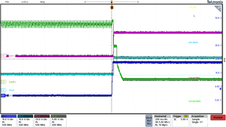
    Diagrams BATFET with no load, BATFET mode:

    HW.ACUV = 13.6V, VAC_DPM = 13V, VAC = 19V

    Ch1 = battery current (neg. = charge)
    Ch4 = VSYS
    M = VGS BATFET

    no load:

      
    discharge => charge                                                                charge => discharge

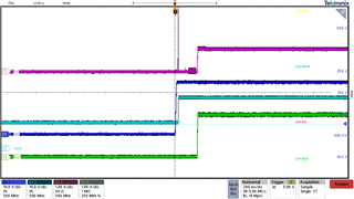
    Diagrams ACFET, auto-reverse mode:

    HW.ACUV = 13.6V, VAC_DPM = 13V, VSYS_REV = 15V, VAC = 19V

    Ch1 = battery current (neg. = charge)
    Ch4 = VSYS
    Ch2 = ACDRV

    no load:

      
    discharge => charge                                                                charge => discharge

    load:


  • I will try to recreate your situation where if there is already a load when Vin is present and then Vin is disconnected, BATFET should turn on but it doesn't as you said. In my current analysis that I have shared with you, there is no problem with a 0.5A load.

  • The target load is up to 3A.

  • I will try until a 5A load and let you know.

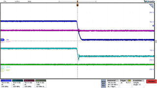
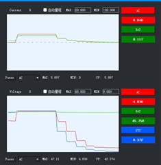
  • Please find attached waveform. It works as expected under VAC = 19V, VOUT = 12V, 3A load current

  •  Hello Utsav Gupta, I represent Günter Bruckmann during his vacation. I built the circuit and made the following measurements:

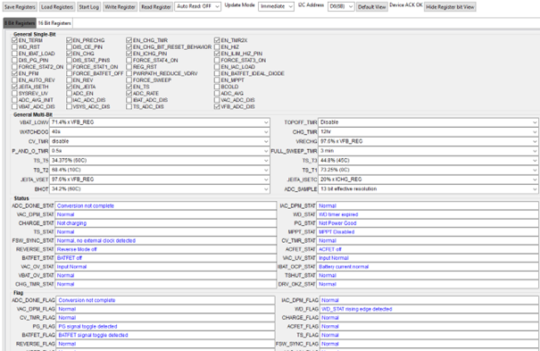
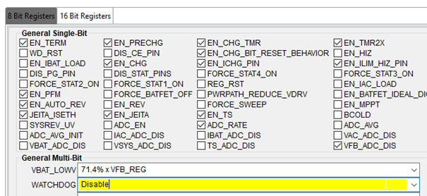
    Register immediately after switching on. Just read, no changes made.


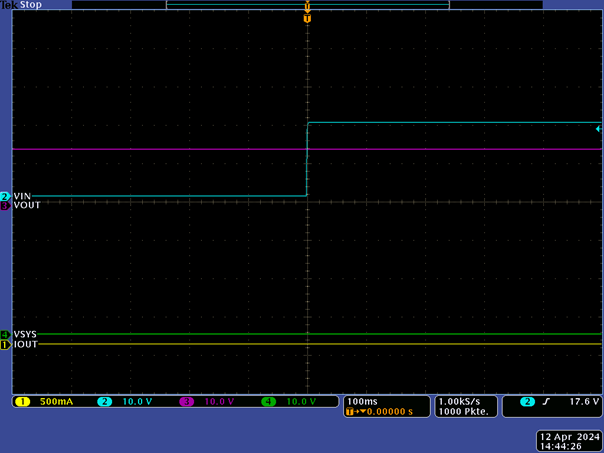
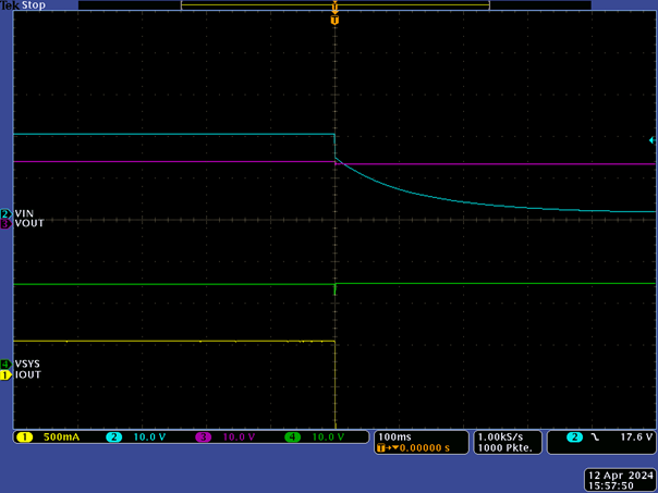
     Even when switching on under load, VSYS remains at 0V and IOUT at 0A.

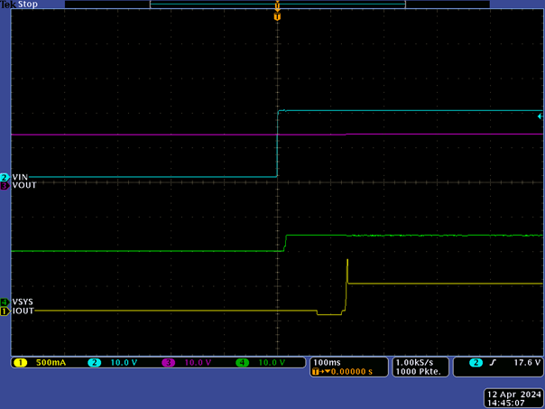
    If you disconnect the load beforehand and then switch on VIN, the following picture occurs when switching on:

    VSYS increases from 14.8V (approx. VBAT) to 19V. IBAT from 0 to 377mA. IIN = 339mA.

    When the load is switched on, IIN increases to 1,444 A. IBAT increases slightly to 384mA.


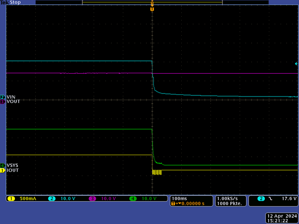
     If the operating voltage is switched off under load, VSYS drops to 0V and IOUT to 0A.

    If you remove the load, VSYS increases again to 19V and the charging continues at 377mA.

    If EN_AUTO_REV is activated and WATCHDOG is deactivated and the operating voltage with load is switched off, the following picture results:


     Vin drops, VSYS drops from 19V to 5V. The battery is loaded with 113 mA.


    If VSYS_REV is set to 19V, the following picture results:


     Vin drops, VSYS stays at around 19V. The battery is loaded with 1.6A. IOUT becomes negative because the battery is stressed in this mode.

    Was the circuit operated in reverse mode in your setup?


  • Hi Thomas,

    The ciruit was NOT operated in reverse mode. Watchdog timer always has to be disabled before you start charging/switching. That is the first step irrespective of forward or reverse mode. Let me explain my test procedure to you with which I obtained my latest graph.

    Connect DC supply to Vin. Connect DC load to SYS. Connect battery simulator to Vout, turn on and provide desired voltage. Read registers, disable watchdog timer. Set desired ICHG. Then turn on DC supply to Vin with the desired voltage. The device status should say charging ex. fast charge. The device status should day ACFET on BATFET off. Then turn on DC load with constant current of 3A (or whatever is desired). The total input power on the DC supply should be same as the total output power. Set up the scope to single capture and trigger at Vin falling edge. Then turn the VAC off. BATFET should turn on smoothly and Vsys should change from Vin level to Vout level and Iout should remain same as battery is providing the load.

    Please let me know if you followed the same procedure. If not, please try this procedure and send me the results of what you see. No reverse mode needed.

  • Hi Utsav,

    Unfortunately it behaves like “If the operating voltage is switched off under load, VSYS drops to 0V and IOUT to 0A.” when I use the same procedure as you described.

    As described at the beginning of the chat, we unfortunately had to convert a BQ25756 EVAL board for use as a BQ25750 board because no other EVAL boards were available at the moment.

    Would it be possible that there is still a difference between the two board variants that is not documented?

    I just received news that the correct EVAL board is now available again. We will now order the correct EVAL board and repeat the experiments. I will then report on the results.

    Thank you!

  • Hi Thomas,

    We are making some bit changes in our IC that may enable better power path transfer. These changes are experimental right now and not final. The graph I sent you was obtained after making those changes., Maybe that is why you are still seeing failure.

    Unfortunately the EVM was out of stock for a few days but is back in stock now. Please send me the results on the latest EVM. I will also try to finalize the experimental bit changes by then and then hopefully we can close this issue.

  • Hello Utsav,

    Unfortunately the new board doesn't behave as expected either. As soon as you turn off VIN while the load is connected, VSYS drops to zero. After switching on VIN with the load connected, the LED for PG only flashes briefly cyclically. If you switch the load after changing the supply from VIN to battery supply, the board works normally. With VIN, the set current is delivered to the battery and the load is supplied with power normally. If you subsequently switch on the load in battery operation, the load is fed from the battery as expected. Even if I leave the jumpers for current and voltage limitation as they were when delivered, I get the same result. As in all previous experiments, the watchdog was switched off.

    I took a look at the chip housing.

    The old chip says:

    BQ25750

    TI 3C8

    A05T G4


    The new chip says:

    BQ25750

    TI 3A8

    AF63 G4

    Is this the new batch you used too?

    If not, where can we get the newer chips and how can you tell that you are ordering the right ones?

    Best regards, Thomas

  • Hi Thomas, there are no newer BQ25750 chips. The ones you have should be okay. There has been no revision since release so nothing has changed between different batch of ICs. As I mentioned before, the reason you are seeing failure and I am not is because I am using some experimental settings in my registers which are usually not accessible to the user and set at the factory. I think that will definitely solve your issue once we finalize those settings. Until then, could you please try power path transfer with a load of less than 10W at the output. For example input voltage 20V battery voltage 15V load current 0.5A. I know that this is not the condition you desire but I just want to make sure the board you are using is okay. Power path transfer should be successful at lower loads.

  • Hi, Utsav!  I met the same problem with Thomas.

    I Bought BQ25750IC From DigiKey.

    I test Input voltage 48V Battery voltage 12S(48V),Load current 0.5A,Power path transfer work OK;

    I test Input voltage 48V Battery voltage 12S(48V),Load current 1.0A,Power path transfer work Fail;Vsys and Vac Drop.BatFet try Open Again and Again;

  • Hello Utsav,

    I gradually increased the ohmic value of the load resistor. The circuit works under 330 mA load current. This corresponds to a load resistance of 49 ohms (14.7V / 0.3A) and an output power of 4.41W (14.7V * 0.3A). When switching off, there is a complete drop in the VSYS voltage. Regardless of whether the watchdog mode is switched on or off, the output voltage drops for approx. 10ms. I even saw a voltage drop lasting 60ms without load.

    When switching on, there is a nice, smooth transition of the VSYS voltage from VBAT to VAC without load. After approx. 115 ms the battery takes over, which can be recognized by an overshoot of the battery current.

    The situation is very similar with load; the charging current logically immediately drops to zero. The current from VAC is also taken over after approx. 115 ms.

    In our project we want to provide 15W. With a capacitor of approx. 150µF we could theoretically feed the power of 15W from the capacitor at approx. 15V for approx. 1.12ms (0.5*150e-6AS/V*15V^2/15VA). Since the voltage cannot drop far, we have to assume closer to 0.1 ms. This would be the time after which the battery would have to take over at the latest.

    Best regards

    Thomas

  • Hi Thomas and the other person (???),

    I am now sure that the problems you are seeing can be resolved by changing some hidden bits not accessible to the customer. These bits are set at the factory and hence this problem will most likely only go away when you order the new ICs with the updated trim and OTP settings. In the meanwhile, I request you to try one last thing. Program your ACUV higher than VBAT and lower than VAC obviously. For example if your VAC is 28V and VBAT is 20V, please program your ACUV to 22V for example. Some of our customers have done that and received much better results. Please let me know if that makes a difference.

  • Hello Utsav,

    I chose R21 = 2.4 Meg, R27 = 133K, R30 = 25.5K. This results in ACUV = 17.756V.

    RFBG = 33R, RTOP = 249K, RBOT = 25.5K (2 x 51K II). It follows that VBAT = 16.554V.

    The charging process only begins when the voltage is greater than VAC = 20V.

    The dip in VSYS remains as before, about ½ UBAT for about 20 ms. The circuit only works up to a load current of
    approx.330 mA.

    When switching on, there is still a nice, smooth transition of the VSYS voltage from VBAT to VAC under load. The battery takes over after approx. 15 ms.

    Best regards

    Thomas

  • Hello Utsav,
    I noticed that pin 17, MODE, in the EVAL board, is connected to ground by over 3k. According to the data sheet, the pin should be connected directly to ground. An attempt to switch the pin to ground with a smaller resistor (120 ohms) resulted in no change. What is the function of the pin?

  • Hi Thomas, if there is still no improvement in your results if you use a higher ACUV than the VBAT, I think only an IC revision with the new bit settings we tested internally will solve this problem.

    Pin 17 is just the PGND (ground pin).

  • Hello Utsav,

    can you tell me whether the IC revision with the new bit settings is already available?

    If not, when will we be able to get them?

    What must be written on the chip if it is a new IC revision?

    The name of the components shouldn't even have to change, because the revision of the components is usually not specified by the distributors. Would there perhaps be a way to send us samples, because we need to make progress on our project as quickly as possible? Could you perhaps send me a link where I can order the current components?


    Thank you!

  • Hi Thomas,

    Unfortunately at this time, we cannot provide a timeline for samples or when the revised IC will be released.