This thread has been locked.

If you have a related question, please click the "Ask a related question" button in the top right corner. The newly created question will be automatically linked to this question.

TPS25751: PTCH mode update fails

Part Number: TPS25751
Other Parts Discussed in Thread: TPS25730,

USB Type C team,

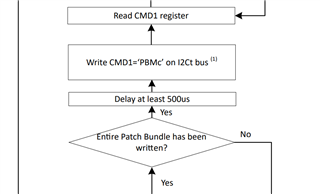
Our customer is using TPS25751 on the power Source side, and a TPS25730 on the Sink side.  When configuring the TPS25751, they read the mode register and get PTCH, indicating they need to apply the patch update.  They follow the steps in the flow chart in Figure 5-1 of the TRM.  They get to the diamond in the bottom left where they expect to read DATA1=0 for success, but they always read 0x05.

Can you give advice on how to debug this so they can get to APP mode?

Thanks,
Darren

  • Hi Darren,

    Thank you for your query, we have received your request. Please give our team some time to look at this and we will provide a response in the next few days.

    Thank you for your patience as we work through a high intake of E2E posts.

    Best,

    USB-C/PD Team

  • Hi Darren,

    Thanks for reaching out!

    Can you please ask the customer how long they take to send the PTc command?

    It should be set to roughly 40ms. We have had customers send the patch complete command to the PD quicker than that causing the PD to remain in patch mode.

    Thank you,

    Kevin Kosta

  • Hi Kevin,

    I don't have the answer to the time delay on PTc yet.  Which step in the flow chart is sending the PTc command?

    The customer sent me additional questions about what to send when applying the patch in Table 4-12.

    Please confirm that the end goal is to setup the TPS25751 in APP mode to make it operate.

    After reading PTCH, they start through the flow chart.

    They read Interrupt Mask register(0x16):

    ReadyForPatch bit = 1, and the all value of this register is: 0x02 0x00 0x00 0x00 0x00 0x00 0x00 0x00 0x00 0x00 0x00

    Then they write the Data register (0x09):

    0x00 0x08 0x08 0x08 0x08 0x20 0x32 0x00 0x00 0x00 0x00 0x00 0x00 0x00 0x00 0x00 0x00 0x00 0x00 0x00 0x00 0x00 0x00 0x00 0x00 0x00 0x00 0x00 0x00 0x00 0x00 0x00 0x00 0x00 0x00 0x00 0x00 0x00 0x00 0x00 0x00 0x00 0x00 0x00 0x00 0x00 0x00 0x00 0x00 0x00 0x00 0x00 0x00 0x00 0x00 0x00 0x00 0x00 0x00 0x00 0x00 0x00 0x00 0x00

    What should they be writing for the "Bundle Size"?

    What should they write in Target Address in the bits 6:0 as in Table 4-12?  Should it be the I2C address of the SINK side TPS25730?

    Thanks,

    Darren

  • Hi Darren,

    This is the section of the flow chart that I was referring too. If the customer sends it out at 500us we will likely see the PD stay in patch mode.

    But this step would occur after reading 0 from the DATA1 register.

    Give me a couple of hours and I will grab an I2C example capture of the PD being booted by an EC that should help here.

    Thank you,

    Kevin

  • Hi Darren,

    Please see the attached saleae log!

    https://e2e.ti.com/cfs-file/__key/communityserver-discussions-components-files/196/TPS25751_5F00_PBMx_5F00_BOOT.sal

    Thank you,

    Kevin