This thread has been locked.

If you have a related question, please click the "Ask a related question" button in the top right corner. The newly created question will be automatically linked to this question.

BQ76952: Current Calibiration issue on 500uOhm Shunt

Part Number: BQ76952
Other Parts Discussed in Thread: BQSTUDIO

Dear All,

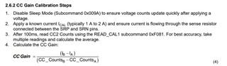
We are using BQ7695203 with a 500uOhm shunt, As per the datasheet after setting the

CC Gain to CC Gain = 7.4768 / (Rsense in mOhm) 

CC Gain = 7.4768 / 0.5 = 14.9536 

and

Capacity Gain = Calibration:Current:CC Gain x 298261.6178

Capacity Gain = Calibration:Current:14.9536  x 298261.6178 = 44,60,084.9279

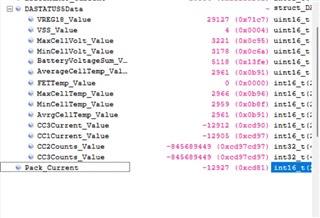
Not getting the accurate current at the time of CC2 Counts reading. The actual current on the clamp meter is 26.3Amp and we are getting from AFE is 13421mA. 

Measurement interval time from AFE is 500mSec.

Please help us with what other parameters or settings should we set to get the accurate current. 

  • Hello Raja,

    The actual CC gain equation should be CC Gain = 7.5684 / (Rsense in mΩ) = 7.5684/0.5 = 15.1368.

    Capacity Gain = Calibration:Current:CC Gain x 298261.6178 = 4,514,726.456

    These are shown in Section 4.12 Current Calibration of the TRM. Now, I am surprised that the measurement is that large. Do you see any difference in CC1?

    You can also perform calibration by following the steps in Section 2.6 Current Calibration of the BQ769x2 Calibration and OTP Programming Guide. Do you see any improvement if you calibrate this way?

    Best Regards,

    Luis Hernandez Salomon

  • Hello Luis,

    Thanks for the reply. I will above task, need help also, CC Gain and Capacity Gain both are in F4 32-bit IEEE-754 floating point format. So can you please confirm the below function to write this value in this format?

    In the below function, datalen will be 4 then case 4 will work please check and confirm to move ahead.

    #define CCGain 0x91A8 //Calibration:Current:CC Gain
    #define CapacityGain 0x91AC //Calibration:Current:Capacity Gain

    // Current Calibiration.
    BQ769x2_SetRegister_f(CCGain, CC_GainValue, 4);

    // Current Calibiration.
    Capacity_GainValue = CC_GainValue * 298261.6178;
    BQ769x2_SetRegister_f(CapacityGain, Capacity_GainValue, 4);

    void BQ769x2_SetRegister_f(uint16_t reg_addr, float reg_data, uint8_t datalen)
    {
    uint8_t TX_Buffer[2] = {0x00, 0x00};
    uint8_t TX_RegData[6] = {0x00, 0x00, 0x00, 0x00, 0x00, 0x00};

    uint32_t* Pointer = (uint32_t*)&reg_data;
    //TX_RegData in little endian format
    TX_RegData[0] = ((*Pointer) & 0xff);
    TX_RegData[1] = (*(Pointer+1) & 0xff);
    TX_RegData[2] = ((*Pointer) & 0xff); //1st byte of data

    switch(datalen)
    {
    case 1: //1 byte datalength
    SPI_WriteReg(0x3E, TX_RegData, 3);
    delay_ms(2);
    TX_Buffer[0] = Checksum(TX_RegData, 3);
    TX_Buffer[1] = 0x05; //combined length of register address and data
    SPI_WriteReg(0x60, TX_Buffer, 2); // Write the checksum and length
    //delay_us(2000);
    delay_ms(2);
    break;
    case 2: //2 byte datalength
    TX_RegData[3] = (*(Pointer+1) & 0xff);
    SPI_WriteReg(0x3E, TX_RegData, 4);
    //delay_us(2000);
    delay_ms(2);
    TX_Buffer[0] = Checksum(TX_RegData, 4);
    TX_Buffer[1] = 0x06; //combined length of register address and data
    SPI_WriteReg(0x60, TX_Buffer, 2); // Write the checksum and length
    //delay_us(2000);
    delay_ms(2);
    break;
    case 4: //4 byte datalength, Only used for CCGain and Capacity Gain
    TX_RegData[3] = (*(Pointer+1) & 0xff);
    TX_RegData[4] = (*(Pointer+2) & 0xff);
    TX_RegData[5] = (*(Pointer+3) & 0xff);
    SPI_WriteReg(0x3E, TX_RegData, 6);
    //delay_us(2000);
    delay_ms(2);
    TX_Buffer[0] = Checksum(TX_RegData, 6);
    TX_Buffer[1] = 0x08; //combined length of register address and data
    SPI_WriteReg(0x60, TX_Buffer, 2); // Write the checksum and length
    //delay_us(2000);
    delay_ms(2);
    break;
    }
    }

  • Hi Luis, I tried to read DASTATUS5(), please check the image of all data after the above-suggested configuration.

    In below images Pack_Current is reading of CC2 register and other DASTATUS5(). The actual current was flowing 25 Amp but getting below values. 

    And other you suggested calibrating the BMS BQ769x2 Calibration and OTP Programming Guide. In that,I need to know what are IB, IA, CC Count B, and CC Count A.


    Please help us how we can resolve this current-related issue.

  • Hello Raja,

    Section 2.9.1 Code Example of the same application guide shows an example code for the calibration procedure. That may be useful to see.

    Ib, Ia are known current values that you would apply. So, if you apply a known current that would be one point, then you can apply the second known current and that would be Ib. While reading Ia you would read the CC_Counts for each current respectively. Then put these in the equation. The CC counts you can get.

    Best Regards,

    Luis Hernandez Salomon

  • Dear Luis,

    Thanks for the reply. Fine below thing.

    After writing I tried to read both values but got the same as default, which means the values are not changing. there are some issues in the writing process.

    Below is the process I am following, please help me if I am doing anything wrong. Below is the complete Init Function

    void BQ769x2_Init(void) {
    // Configures all parameters in device RAM

    // Enter CONFIGUPDATE mode (Subcommand 0x0090) - It is required to be in CONFIG_UPDATE mode to program the device RAM settings
    // See TRM for full description of CONFIG_UPDATE mode
    CommandSubcommands(SET_CFGUPDATE);

    // After entering CONFIG_UPDATE mode, RAM registers can be programmed. When programming RAM, checksum and length must also be
    // programmed for the change to take effect. All of the RAM registers are described in detail in the BQ769x2 TRM.
    // An easier way to find the descriptions is in the BQStudio Data Memory screen. When you move the mouse over the register name,
    // a full description of the register and the bits will pop up on the screen.

    // 'Power Config' - 0x9234 = 0x2D80 //9E0
    // Setting the DSLP_LDO bit allows the LDOs to remain active when the device goes into Deep Sleep mode
    // Set wake speed bits to 00 for best performance
    BQ769x2_SetRegister(PowerConfig, 9E0, 2); //Power Config

    // 'REG0 Config' - set REG0_EN bit to enable pre-regulator
    //BQ769x2_SetRegister(REG0Config, 0x01, 1); // doubt

    // 'REG12 Config' - Enable REG1 with 3.0V output (0x0B for 3.0V, 0x0F for 5V)
    BQ769x2_SetRegister(REG12Config, 0x0B, 1);
    BQ769x2_SetRegister(REG12Config, 0x0F, 1);

    // Set CFETOFF pin to Config (AFE_CS to oin enable)
    BQ769x2_SetRegister(CFETOFFPinConfig, 0x4A, 1);

    // Set DFETOFF pin to measure Cell Temperature - 0x92FB = 0x87 (set to 0x00 to disable) // set TS4 to measure cell temperature
    BQ769x2_SetRegister(DFETOFFPinConfig, 0x07, 1);

    // Set up ALERT Pin - 0x92FC = 0x2A // 0x22
    // This configures the ALERT pin to drive high (REG1 voltage) when enabled.
    // The ALERT pin can be used as an interrupt to the MCU when a protection has triggered or new measurements are available
    // The Alert pin to measure Data ready
    BQ769x2_SetRegister(ALERTPinConfig, 0x22, 1);

    // Current Calibiration.
    BQ769x2_SetRegister_f(CCGain, CC_GainValue, 4);

    // Current Calibiration.
    Capacity_GainValue = CC_GainValue * 298261.6178;
    BQ769x2_SetRegister_f(CapacityGain, Capacity_GainValue, 4);

    Subcommands(CCGain, 0x00, R);
    Subcommands(CapacityGain, 0x00, R);

    // Set TS1 to measure Cell Temperature - 0x92FD = 0x87 //0x87
    BQ769x2_SetRegister(TS1Config, 0x07, 1);

    // Set TS2 to measure Cell Temperature - 0x92FE = 0x87
    BQ769x2_SetRegister(TS2Config, 0x07, 1);

    // Set TS3 to measure Cell Temperature - 0x92FF = 0x87
    BQ769x2_SetRegister(TS3Config, 0x07, 1);

    // Set HDQ to measure Master Otuput Slave Input - 0x9300 = 0x00
    BQ769x2_SetRegister(HDQPinConfig, 0x00, 1); // No thermistor installed on EVM HDQ pin, so set to 0x00

    // Set DDSG TO measure short circuit detection
    BQ769x2_SetRegister(DDSGPinConfig, 0xA2, 1);

    // 'VCell Mode' - Enable 16 cells - 0x9304 = 0xFFFF; Writing 0xFFFF sets the 16 cells
    BQ769x2_SetRegister(VCellMode, 0xFFFF, 2);

    // Set up Protection Configuration Register Field Descriptions Disable all
    BQ769x2_SetRegister(ProtectionConfiguration, 0x0000, 2);

    // Enable protections in 'Enabled Protections A' 0x9261 = 0xBC
    // Enables SCD (short-circuit), OCD1 (over-current in discharge), OCC (over-current in charge),
    // COV (over-voltage), CUV (under-voltage)
    BQ769x2_SetRegister(EnabledProtectionsA, 0x80, 1);

    // Enable all protections in 'Enabled Protections B' 0x9262 = 0xF7
    // Enables OTF (over-temperature FET), OTINT (internal over-temperature), OTD (over-temperature in discharge),
    // OTC (over-temperature in charge), UTINT (internal under-temperature), UTD (under-temperature in discharge), UTC (under-temperature in charge)
    BQ769x2_SetRegister(EnabledProtectionsB, 0x00, 1);

    // Enable protections in 'Enabled Protections C' 0x9263 = 0x4F
    BQ769x2_SetRegister(EnabledProtectionsC, 0x41, 1);

    // 'Default Alarm Mask' - 0x..82 Enables the FullScan and ADScan bits, default value = 0xF800
    BQ769x2_SetRegister(DefaultAlarmMask, 0xF882, 2);

    // Set up Cell Balancing Configuration - 0x9335 = 0x03 - Automated balancing while in Relax or Charge modes
    // Also see "Cell Balancing with BQ769x2 Battery Monitors" document on ti.com
    BQ769x2_SetRegister(BalancingConfiguration, 0x03, 1);

    BQ769x2_SetRegister(CellBalanceInterval, 0x05, 1); //Cell Balance Interval 5 Seconds
    BQ769x2_SetRegister(CellBalanceMaxCells, 0x05, 1); //Cell Balance Max Cells 5 Cells

    BQ769x2_SetRegister(CellBalanceMinCellVCharge, 0x0CE4, 2); //Cell Balance Min Cell V (Charge) 3300mV
    BQ769x2_SetRegister(CellBalanceMinDeltaCharge, 0x1E, 1); //Cell Balance Min Delta (Charge) 30mV
    BQ769x2_SetRegister(CellBalanceStopDeltaCharge, 0x0F, 1); //Cell Balance Stop Delta (Charge) 15mV

    BQ769x2_SetRegister(CellBalanceMinCellVRelax, 0x0CE4, 2); //Cell Balance Min Cell V (Relax) 3300mV
    BQ769x2_SetRegister(CellBalanceMinDeltaRelax, 0x1E, 1); //Cell Balance Min Delta (Relax) 30mV
    BQ769x2_SetRegister(CellBalanceStopDeltaRelax, 0x0F, 1); //Cell Balance Stop Delta (Relax) 15mV


    // Set up CUV (under-voltage) Threshold - 0x9275 = 0x31 (2479 mV)
    // CUV Threshold is this value multiplied by 50.6mV
    BQ769x2_SetRegister(CUVThreshold, 0x31, 1);

    // Set up COV (over-voltage) Threshold - 0x9278 = 0x55 (4301 mV)
    // COV Threshold is this value multiplied by 50.6mV
    BQ769x2_SetRegister(COVThreshold, 0x55, 1);

    // Set up OCC (over-current in charge) Threshold - 0x9280 = 0x05 (10 mV = 10A across 1mOhm sense resistor) Units in 2mV
    BQ769x2_SetRegister(OCCThreshold, 0x05, 1);

    // Set up OCD1 Threshold - 0x9282 = 0x0A (20 mV = 20A across 1mOhm sense resistor) units of 2mV
    BQ769x2_SetRegister(OCD1Threshold, 0x0A, 1);

    // Set up SCD Threshold - 0x9286 = 0x05 (100 mV = 100A across 1mOhm sense resistor) 0x05=100mV // 0x02=40 mV(31mV)
    BQ769x2_SetRegister(SCDThreshold, 0x02, 1);

    // Set up SCD Delay - 0x9287 = 0x03 (30 us) Enabled with a delay of (value - 1) * 15 µs; min value of 1
    BQ769x2_SetRegister(SCDDelay, 0x01, 1);

    // Set up SCDL Latch Limit to 1 to set SCD recovery only with load removal 0x9295 = 0x01
    // If this is not set, then SCD will recover based on time (SCD Recovery Time parameter).
    BQ769x2_SetRegister(SCDLLatchLimit, 0x01, 1);


    // Exit CONFIGUPDATE mode - Subcommand 0x0092
    CommandSubcommands(EXIT_CFGUPDATE);
    }

  • Hello Raja,

    I would suggest that you use an online calculator for the IEEE-754 to confirm if your code is correctly converting it. I'd also make sure that your checksum and length is being properly done. A logic analyzer capture sequence would help me confirm that for you.

    This older E2E ran on a similar issue:

    https://e2e.ti.com/support/power-management-group/power-management/f/power-management-forum/1346253/bq76952-problems-programming-calibration-current-cc-gain-register

    The checksum in this case was not correct.

    Best Regards,

    Luis Hernandez Salomon

  • Resolved, I was using the wrong register value at the time of transmitting data. Thanks for the Big support.