Other Parts Discussed in Thread: LM5156
Greetings, I hope somebody could help me. I'm trying to design a SEPIC converter based on LM3478, with input voltage range 12-36V, and output 24V 2A. I'm calculated all relevant values of components, according to "AN-1484 Designing A SEPIC Converter" and LM3478 Datasheet, and the results was quite similar with examples provided, also I tried to use Webench, but its values we're far beyond mine and example's, so I ignored it. Anyway, after the assembly, I'm stuck with the problem, that converter holds output voltage at +/- 24V, but under load of 1.8 A (LED driver at the output holds current), both of inductors and mosfet quickly overheating, in, like, 30 seconds. In this way I burned two mosfets, because I haven't noticed, that diode became shorted in some reason too, so, I changed mosfet, and burned second one. Also, I noticed that in case of input voltage is 24V and more(buck mode), with no load, mosfet heats in pulses (like, sharply became hot, and then cooling down and repeat), and current on my lab power supply synchronously jumps to 0.2-0.3 A and goes back to zero (I havent's noticed this effect in boost mode, when VIN lower than 24V). So, here is the question, is there root of problem in poor PCB design, or there is some fundamental miscalculation, that I don't see? I re-read different datasheets and appnotes, and many topics on forum, but I still haven't clear solution.
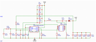
Here's schematic, L1 and L2 have L=10 uH, DCR=30 mOhm, Irms=7.8A, Isat=8.5A, MOSFET is Infineon BSC0702LS.
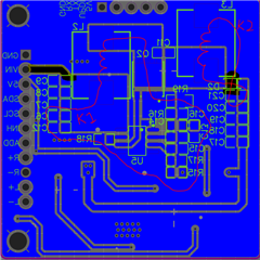
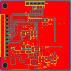
And PCB (all layers)
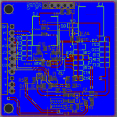
PCB's bottom (SEPIC located here)
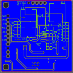
PCB's top (here located LED driver, opamp and MCU)
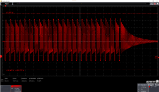
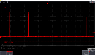
Waveform of L2 (input inductor) at 21.7V. If I'm lowering the input voltage on lab supply, quantity of pulses rising, and if I'm increasing input, pulses count becaming lower until 24V, and after switching to buck mode, I assume, increasing again (and in buck mosfet starting to overheat, with no load).
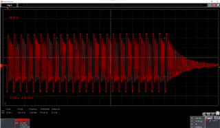
Waveworm of L3 (output inductor), same behaviour.
MOSFET gate, same behaviour
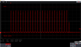
Gate on 24 V input
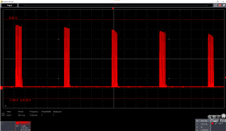
Gate on 26 V input
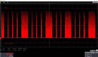
Gate on 28 V input
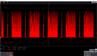
Gate on 30 V input
I'm wondering, why in boost mode, when VIN < 24 V, quantity of pulses on gate increasing and decreasing slowly, but after VIN > 24 V it became superfast, like increasing VIN for 0.1 V doubles the pulses count.
Thank you in advance,
Ihor Ziuba.