This thread has been locked.

If you have a related question, please click the "Ask a related question" button in the top right corner. The newly created question will be automatically linked to this question.

LM25183-Q1: Unable to get a regulated output for my power converter.

Part Number: LM25183-Q1
Other Parts Discussed in Thread: LM25183, LM25184

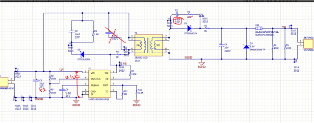
Hi, I am using the LM25183-Q1 to get 5V at the output with inputs ranging from 9V to 20V. I used the design sheet given by TI to calculate the inductance and all the passive components for my design. The inductance calculated by the design sheet for me is 8 uH for a 2:1 transformer while I used a 2:1 - 14 uH coilcraft ZB1052-AE which is the recommended transformer in the datasheet.

Here is the screenshot of the design sheet that I used to build my prototype.

The built prototype is not regulating the output voltage. Also I see it going unstable as it keeps going back and forth between the Boundary conduction mode and the frequency fold-back mode while in steady state. I can also see that on a few occasions the mosfet is turned on even though the current on the secondary has not went down all the way to 0. As of now I have built this prototype using a breakout board and a perf board, so the layout is not super clean.

I have also attached my schematic in this message for your reference. Can you please help me fix the problem?

Regards

Chinmay

  • Hi Chinmay,

    Thank you for designing with the LM25183.  The main problem I think is in your circuit board.  You should build a clean PCB other than using a perf board. The noise would affect the performance. 

    I understand that you want to verify the basic performance first before spending much time on design a PCB. Here I recommend you to order our EVM.  You should order and LM25184 EVM (link below), and replace the IC with the LM25183, and change the transformer to your selection, and also make other components to be the same as your already decided. After doing these, you will see that your design works well on our EVM layout.

    https://www.ti.com/tool/LM25184EVM-S12

    Regarding your calculator picture, I think you did right with it. 

    Regarding your schematic, you may consider to make the following change:

    • Delete 0.1nF capacitor across the primary winding. 
    • Install a 0.1uF across VIN and GND, placing beside the IC.
    • Delete C1 and R1 snubber:  0.1uF and 10k are too big. The snubber values can be decided after test.  However, for your initial test, they can be left open.
    • You may consider to add another 22uF across the input rail.  
    • Note that, either use our EVM board, or design your PCB by following the layout guideline presented in the datasheet, and referring to the EVM board layout example.  This is very important to get a good design to work well.  

    Best Regards,

    Youhao

  • Thank you Youhao,

    I have ordered the evaluation board. I will make the changes on that and keep you posted on the results. Thank you.

    Regards

    Chinmay 

  • Hi Chinmay,

    Thank you!  I am looking forward to your updates.  Good luck!

    Best Regards,

    Youhao