This thread has been locked.

If you have a related question, please click the "Ask a related question" button in the top right corner. The newly created question will be automatically linked to this question.

LM5122: SW output failing

Part Number: LM5122

There was already a similar issue reported with the same title. We have faced out SW node short to AGND. What could cause this? Here are some design infos:

We are using the LM5122Z as a boost converter to provide ca. 66V at max. 0.8A (ca. 50W output power) for an input voltage range between 18-33V (typical) respectively 12 - 40V (emergency for some tens of seconds). The switching frequency is ca. 210kHz.

The fail occured at the following condition: input voltage raised to 51V, which triggers our own voltage monitor and disables the LM5122 via the UVLO pin (tie to low). During my observation the SW node fail occured if we reduced the voltage down to ca. 49V , which enables the LM5122 again. I obsereved strange acoustic noise from power components converter. After input power switch off we noticed the SW node short to AGND.

We have an input voltage transient limiter, which limits the input voltage to 53 - 54V in any case independend what the input transient is. So input voltage is well below any maximum ratings (e.g VIn or CSP SCN pin etc).

On another board with similar design we heave faced out no issues so far. I have also measured teh SW node via scope during this scenario - so captured first switching pulses at SW node after LM5122 re-enable (going below our own OVLO release threshold of ca. 49V). Is there a possibility that at some circumstances the input voltage is added onto the output voltage. From my understanding this behaviour is not expected for a boost converter., since the converter switch is on Low side.

I can double check with another board but would like to avoid to kill too many LM5122 with this kind of test. Therefore I would like to know theoretically the possible reason for the device fail.Therfore my dedicated questions.

Q1: How sensitive is the SW node to transients

Q2: what are the proper means to reduce transient overshoot at SW node w/o impacting efficiency.

         -> I guess I will not have any issue with the -5V rating since the body diode of the low side MOSFET clamps to about -1V

Q3: is the damage on SW node only a side effect and caused by overvoltage to another pin

Regards Andreas

  • Hello Andreas,

    Thank you for using E2E. Can you please provide the schematic of your design? Can you also please attach the scopeshots from your measurements when the device gets damaged?

    I am looking forward for your response.

    Best regards,

    Moritz

  • Hello Moritz,

    sorry for late reply. Unfortunately I have some issues to provide the schematics here within the forum. The booster stage itself is similar to my webbench design:

    https://webench.ti.com/appinfo/webench/scripts/SDP.cgi?ID=01FD7B3998E0F996

    Regarding the design differences to the webbench design:

    We have an input voltage monitor (window comparator) which drives the UVLO pin of the LM5122. If input voltage is in range (between 14V and 51V) the UVLO pin is driven High (ca. 3.3V). If the input voltage is out of range the window comparator drives the UVLO pin below 0.4V.

    We have tried to catch the damage case with our second power supply again but could not get it repeated. Measurements have not shown any transients on SW node exceeding the maximum ratings (-5V / +105V).

    I assume, that in this specific condition the overvoltage monitor output started to chatter. Is it possible, that the LM5122 may get damaged by high frequency osillations on UVLO pin? According datasheet there is always a delay before switching if the UVLO exceeds the enable threshold of ca. 1.2V, right?

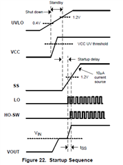
    Section 7.3.7 Soft-Start states the following: "The start-up delay (see Figure 22)
    must be long enough for high-side boot capacitor to be fully charged up by internal BST charge pump."

    What does this mean. Is the start-up delay an device internal delay and what parameter or component values determines this time shown in figure 22?

    Thanks in advance.

    Best Regards,

    Andreas

  • Hi Andreas,

    Thanks for providing additional details.

    There is one question on the input voltage parameters that make it difficult for me to understand the application.
    The input voltage range they set is 18V-33V typical, or 12V-40V in worst case.

    The fail conditions say that the input voltage was 51V.
    Even if the "chatter" effect occurs with UVLO being pulled low and high quickly, this happens at input voltages in the area around 48V-50V, correct?
    This is above the input voltage that was specified specified.

    You are correct that this is still below the abs max of the device, so no device damage is to be expected.
    However, if the design is optimized for VIN 33V max, the regulation may become unstable when operation with 48V.

    Could you explain in further detail why this voltage monitor is implemented on the UVLO pin?
    If Vin goes above Vout, the device would stop switching and go into bypass mode.
    Additionally, if Vin goes above the abs max of the device, the IC would get damaged either way, independent of UVLO being high or low.

    Regarding the startup sequence question,
    when UVLO is pulled low, SS and VCC will start to discharge.
    Pulling UVLO high afterwards will start a new ramp-up sequence including internal delays.
    If SS and VCC did not fully discharge yet, parts of the ramp-up like softstart will be strongly shortened. If Vout did not discharge either, this should not be a problem.
    The BST cap is also charged during the ramp-up sequence. This voltage is required to drive the high side FET.
    But if BST has not discharged either, there will be no problem with turning on the high side FET.

    Thanks and best regards,
    Niklas

  • Hi Niklas,

    thanks for your response. First regarding the input voltage specification. The nominal input voltage is 28 V and the normal range is about 18V to 33V. We have an abnormal range, where our power supply has to operate as well. Therefore, the PSU is designed to operate downto 12V (for 30s) and upto 48V (short term > 51V). Short transients are limited to ca. 53V at power supply input by means of a linear regulator. However, we allow power supply operation only upto ca. 51 - 52 V. Exceeding this voltage (e.g. 60 V or 84 V) will trip our input supply monitor (OVLO) and pull UVLO pin low. This switch-off at ca. 51 V is done to prevent the transient voltage limiter from overload since it is operating as a linear regulator. Under normal operating conditions the transient limiter is acting like a switch (basically no losses other than Rds(on)).

    A second comparator works in the same way for UVLO condition (input voltage below a threshold).

    I have re-done the test after component replacement. I have measured the UVLO as well as the SW node of the booster converter and noticed that after recovery from overvoltage (input voltage decreased slowly downto OVLO release) I could observe that the UVLO pin voltage quickly changed from High to Low. The Low pulse with was some microseconds and the period was the same as the switching period. The SW node voltage has reached high values about 100V and more during the UVLO chattering. I have tried this several times but forgot to save the screenshot and after some trials the LM5122 died again. I try to make new measurements within the next days.

    So the hysteresis of our comparator circuitry seems to be too low as well that we may have an PCB layout issue coupling switching noise to the UVLO line. This is a design issue.

    Nevertheless, I would not expect this kind of behaviour since you mentioned that there is a delay IC internally.

    Q: Could it be possible that there is no delay under certain circumstances (e.g. very short Low pulse of <10us at UVLO Pin?

    Thanks in advance!

    Best Regards,

    Andreas

  • Hi Andreas,

    Thanks for the update and the detailed explanation.
    It is indeed possible that turning the device on and off via UVLO with high frequency can lead to unexpected behavior.
    To avoid this situation, the UVLO has an internal hysteresis which should normally prevent chattering at the UVLO pin, but actively pulling the pin high and low will make the hysteresis useless.

    if the shutdown time of the device is too short, SS cap, VCC cap, etc will not be discharged and it is likely that internal state machines do not react fast enough to put fully put the system into shutdown mode and back into initialization/startup.
    Unfortunately, I have no test data on this, so this theory is based on system design only.

    In general, chattering of UVLO itself should not damage the device. However, if the device is already operated close to the abs max ratings, voltage overshoots due to irregular switching cycles can be a hazards, as your measurements have shown.

    During normal operation, do you already see overshoots or ringing at the SW voltage?
    An effective solution could be to generally reduce voltage overshoots at the SW pin so the design becomes more robust.
    For this, a gate resistances or snubbers can be used.

    Best regards,
    Niklas

  • Hi Niklas,

    Thanks for your informations. I spent another day in the lab to investigate the issue. Basically I got the power supply running w/o damage after I increased  the hysteresis - so no chattering with high frequency anymore.

    Regarding UVLO usage with resistive voltage divider there is also the risk that for low hysteresis the LM5122 may start to chatter at low input line and max. load due to power supply internal voltage drop (e.g. in EMI input filter). I have experienced this with another device in another design. The window comparator gives us more freedom to set the UVLO threshold and UVLO release threshold and in most of the cases the thresholds have tighter tolerance band. Furthermore, it is an existing design, which is not changed.

    I would agree with your statement that chattering at UVLO pin itself should not damage the device. But that is the case and so far I can see from design point of view we are well below maximum ratings.

    We do not have over- undershoots or ringing at the SW node. Currently we are using two MOSFETs in parallel (BSC160N10) with a common 1R gate resistor for Low side and a 10R gate resistor for a single High side MOSFET (same part no). I have already played a bit with the gate resistor of Low side switch MOSFETs and will increase it to ca. 5R. rise time at MOSFET gate is within ca. 20ns. That should be fine.

    I try to make measurements again asap and send you an update with the scope sceenshot from SW node.

    Q: What shutdown time is needed to guarantee that the internal state machines react?

    Best Regards,

    Andreas N.

  • Hi Andreas,

    Thanks for the additional explanation.
    I would highly appreciate additional scope shots where the SW can be seen during the UVLO chattering.

    I will get in touch with a designer in the meantime to understand the internal signal flow of shutdown and UVLO and how long of minimum off-time is recommended.
    I should have an update on this until earlier next week.

    Best regards,
    Niklas

  • Hello Niklas,

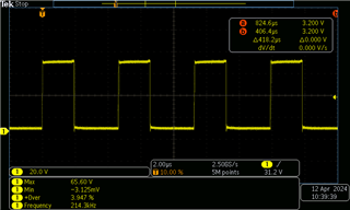
    Unfortunately I have no scope screenshots from UVLO chattering case. Due to hysteresis increase I have no chattering anymore. Nevertheless I send you the switch node waveform during operation as you have asked for in a previous reply. You can see that we have quite clean waveforms. The measurement is done with passive probe and standard ground lead. Input voltage is 28Vdc and Booster ouput voltage is 66V.

    Best Regards Andreas

  • Hi Andreas,

    Thanks for the waveform shot.
    I agree that the system looks stable here and there are no abnormal overshoots.
    I am still waiting for a reply from Design side.

    Please allow me 1-2 additional days to get a reply here.

    Thanks and best regards,
    Niklas

  • Hi Andreas,

    Sorry for the long delay on this.
    I am still waiting for Design to look into this. (Apparently they are under high workload and replies take longer than expected)
    I sent out another mail to push for support with higher urgency.

    I will give you another update by Monday latest.

    Thank you very much for your patience.

    Best regards,
    Niklas

  • Hello Niklas,

    thanks for reporting the actual status. Meanwhile I have studied once again  the datatsheet. In section 7.3.1 I found the following statement:

    "In addition to the UVLO hysteresis current source, a 5-μs deglitch filter on both rising and falling edge of UVLO
    toggling helps preventing chatter upon power up or down."

    Is this somehow directly related to my question regarding state machine minimum pulse length requirement at UVLO?

    Best regards Andreas

  • Hi Andreas,

    Here is the feedback from design:
    It is indeed possible that turn-off/turn-on with high frequency can cause malfunctioning of the device.
    The case of damage at the SW pin due to overvoltage caused by this chattering has not occurred before, so exact cause of this behavior (e.g. state machine glitch) is not fully clear yet and would need further investigation and simulations.

    Regarding the prevention, design recommended to add a hysteresis to the external OVP circuit (just as you already did on your side).
    A minimum hysteresis of 100mV is recommended here. (You can even go up to 200mV to leave extra margin)

    The 5-us deglitch filter from the datasheet you mentioned is a precaution to avoid chattering and glitches at the turn-on and turn-off events, just as you assumed. However, this feature is meant to work in addition to the hysteresis, so both protections should be implemented for a smooth operation.

    Best regards,
    Niklas

  • Hello Niklas,

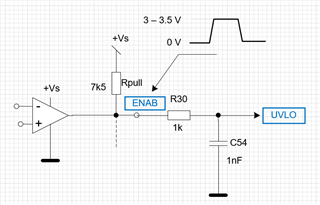
    Thanks for your feedback. I would kindly ask you whether our UVLO control may be an issue. As mentioned we are driving the UVLO via external Comparator as "digital input" rather than as precision enable. Please have a look at attached figure.

    According my simulation the capacitor is counteracting for hysteresis. The 10uA current if UVLO enable threshold is reached does not lead to the desired change in UVLO voltage. For other reasons we have to increase the value of R30 to ca. 22k or higher anyway. According datasheet there is no need for filter capacitor at UVLO input. Am I right? I have checked schematics from EVAL boards. There is sometimes a capacitor implemented (value max. 100pF) . General questions:

    Q1: Does TI allow the usage of a (filter) capacitor at UVLO input? It seems to be as higher the value of C54 the less hysteresis the comparator features. Since we drive it as digital input this shall be no problem. However this  may cause some issue IC internally.

    As a first action we have tried to increase the capacitor value of C54 (ca. 10nF) together with increase of hysteresis of external comparator to cope with our "chatter" and potential damage  issue. This may be the wrong fix.

    Q2: which side effects may a capcitor have? The inbuild comparator has no hysteresis specified other than the enabled current source

    Q3: If capacitor is allowed what shall be the maximum value?

    Actually, I have tested with resistive voltage divider R30=22k, C54=100k and everything works. As far as I can see from datasheet the resistive voltage divider is the right implementation for UVLO pin. The 22k resistor will give us a 220mV hysteresis.

    Many thanks in advance!

    Best regards Andreas

  • Hi Andreas,

    Thanks for the additional notes.

    Q1: Yes, a capacitor can be used at UVLO.

    Q2: A larger cap will decrease the rising/falling slope at UVLO. This would increase the risk of chattering if the voltage would pass the enable/disable thresholds very slowly, but then the internal hysteresis of the IC would become active, so I do not see concerns from device perspective here.

    Q3: There is not maximum value for a capacitor. The driver signal just needs to be strong enough to charge the cap and enable the device.

    Best regards,
    Niklas

  • Hello Niklas,

    many thanks regarding answers to our UVLO control. This helps. Before we can close the ticket I would like to clarify he following two questions popping up according your response:

    "...The case of damage at the SW pin due to overvoltage caused by this chattering has not occurred before, so exact cause of this behavior (e.g. state machine glitch) is not fully clear yet and would need further investigation and simulations."

    Q1: Will this be investigated and followed by TI?

    Q2: In addition to Q1: If you need customer measurements, what are the signals you need (e.g. SW node, UVLO etc.) with focus on which detail regarding voltage thresholds or timing? This is important to get the measurements done BEFORE device damage occurs.

    Q2: What are the proposed means to avoid such situations? Are we on the right track with our measures (increase hysteresis of external comparator, improve PCB layout to avoid cross talk issues)? Do you have any suggestions for UVLO signal filtering / signal conditioning as stated in my last reply?

    The main focus of all this actions is to avoid potential voltage run away at booster output or any unsafe operation leading to potential damage.

    Many thanks for your support so far, I appreciate that. Looking forward to your reply.

    Best regards,

    Andreas

  • Hi Andreas,

    Yes, we will keep investigating into this issue to make sure we understand the root cause and know how to avoid such failure.
    Here it would indeed be helpful if we get additional data on this case so we can simulate more effectively.

    You mentioned it is not possible to share your schematic in the forum, but could you sent it to me via private chat?
    Then we can also perform a general review right away.

    Regarding measurements, it would be helpful to see the UVLO and SW (and optionally VCC and SS) in the situation of a chattering event.
    If I understand correctly, this issue did not re-occur since the hysteresis is in place now so I am not sure if this situation can still be re-created.
    Still, it would be very helpful to know how the UVLO signal behaved when the fail occurred so we can try to re-create this scenario.

    Based on this we can also give more clear recommendations on the UVLO filter/ signal condition to avoid potential failures.

    Best regards,
    Niklas