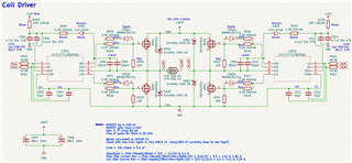
I constructed the following circuit using two UCC27712QDRQ1 driver chips and four IRF150P221 n-channel MOSFETs. I stuck as close as possible to the reference design guidelines, although Cboot may be a bit larger than needed as noted. Bias Vdd in is 12v, common ground. Vhv as tested on the bench was set at 60v, although changing this potential seems to have no significant effect on the high-side voltage.
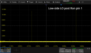
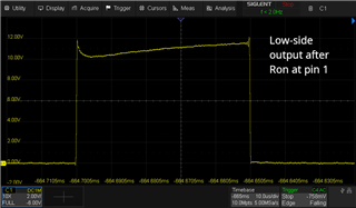
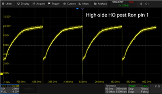
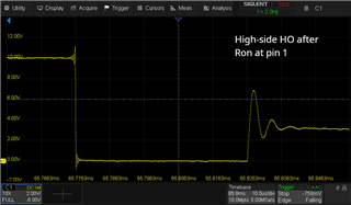
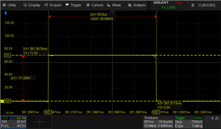
What I am seeing is the expected output when LI is driven high (3.3v) where LO goes from 0v (all DC coupled to common ground) to close to the 12v supply over a single 50uS pulse (spaced at 1 second intervals for testing). What is unexpected (most likely due to my power design ignorance) is that HO is shown with about 10v with HI low until driven high (3.3v) where HO goes to 0v. I expected HO to be around Vhv with HI low, going to Vhv + ~12v when HI is driven high.
Am I misinterpreting the Bias supply input requirements using bootstrap capacitors causing the driver chip to enter some protection mode?
Puzzled, thanks in advance,
Bryan