This thread has been locked.

If you have a related question, please click the "Ask a related question" button in the top right corner. The newly created question will be automatically linked to this question.

LM5122: LM5122MHX LOW SIDE BUCK APPLICATION ISSUE

Part Number: LM5122

Hi 

    I'm Frank 

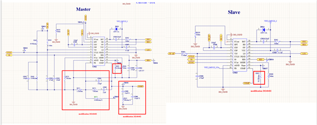
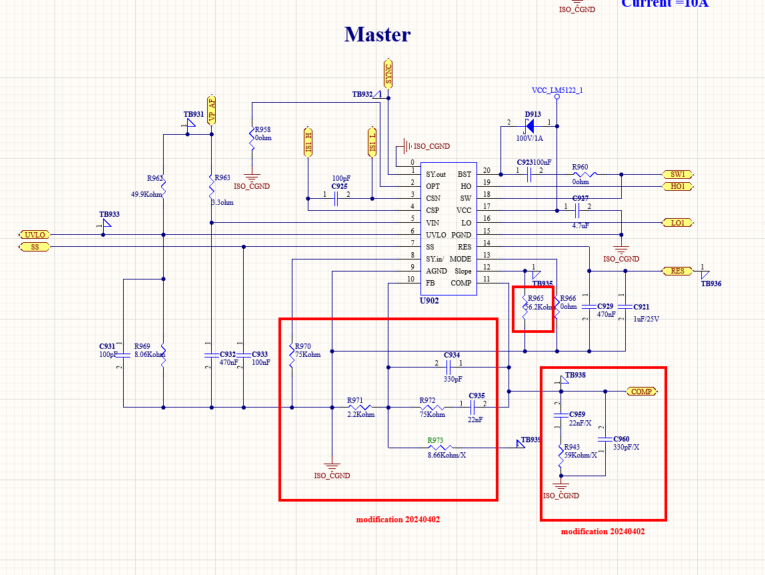
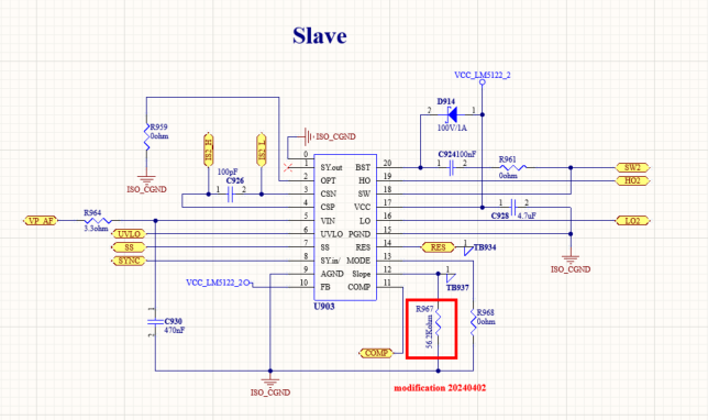
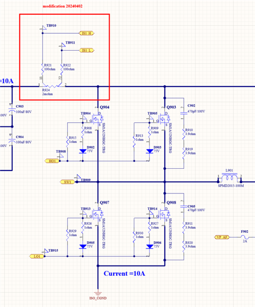
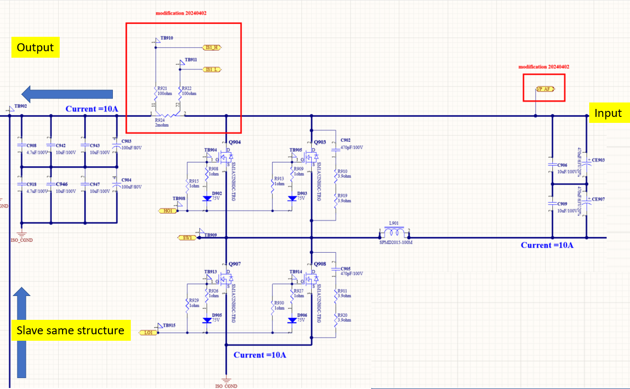
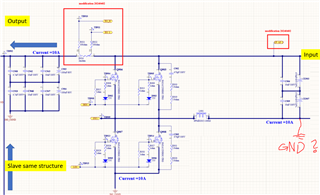
   we met some problem for LM5122MHX used for LOW SIDE BUCK (as custermer requirement as Charger)  Input 56V  output 53.5V/10A

   there is some question below

   1. would you give me some advice if you have experince LM5122MHX on the Low-side buck schematic ?

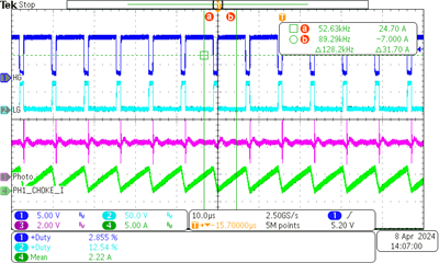
   2. when we use Master schematic W/O Slave it seems could be load to 2A continue (Target is 5A per Phase) , but when we use the 2- phase (Master/Slave),it seem board will Damage 

       but we dont know how...

 So if you have any idea/tips that maybe you could share to us

Below is Master/Slave/Loop/Waveform 


  • BTW, our low side means mosffet is connect to GND-Bus instead V-Bus

  • Hi Frank,

    Thanks for using the e2e forum.
    Unfortunately, my experience with low side buck applications is rather limited.

    From a device perspective, there is one point that caught my attention.
    The sense resistor is located at the input, which means it senses the inductor current only half of the time (when high side FET is closed)
    For a fully functioning sensing, the resistor would have to be located directly at the inductor.
    However, I cannot say for sure yet if this will fully fix the application.

    Would it be possible to share the full schematic section of the power stage?
    Right now I cannot see where the FB trace is connected.

    Thanks and best regards,
    Niklas

  • Hi Niklas

    As we internal discuss, I could update the partial schematic for the Main-Bus schematic with the relative for buck function

     and  combine the slave/master IC part , FB is only in the master/slave part schematic 

    For a fully functioning sensing, the resistor would have to be located directly at the inductor =>

    we discuss internal 

  • Hi Frank,

    Thanks for the update.
    I am very sorry, but I still have trouble fully understanding this power stage.
    Does input side and output side have separate GND connections?
    I can see that the output is connected to ISO_GND. Where is the input side ground connected?

    If they were connected to the same ground level, there would not be any difference between input and output voltage, as they are directly connected.

    I also received feedback from a colleague that the sense resistor should not be placed on the switch note (SW1), as it needs a constant voltage. This means my previous reply is not directly possible.

    Thanks and best regards,
    Niklas