This thread has been locked.

If you have a related question, please click the "Ask a related question" button in the top right corner. The newly created question will be automatically linked to this question.

LM5148: HO, LO mosfet and Inductor is getting heated after connecting a load. Also, switching and HO waveform is distorted

Part Number: LM5148
Other Parts Discussed in Thread: LM5145, LM5149, , LM25149

Hello 

I have designed a dc to dc buck converter of following specs

Input voltage15V to 80V

Output voltage: 12V 10A 

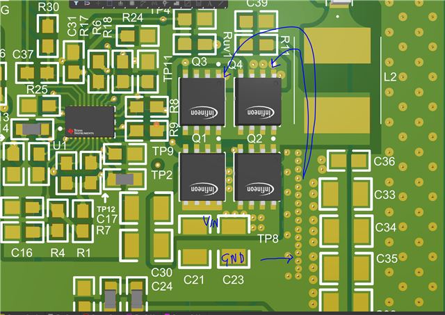
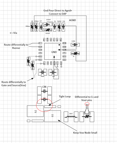
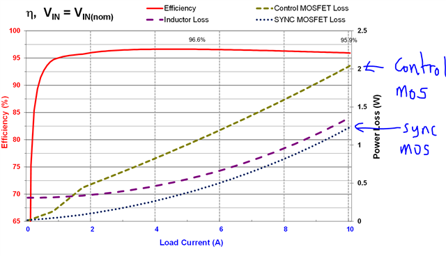
After connecting a load of 7.8A, the waveforms for switching and Ho are all messed up, as you can see in the picture. Along with this both the HO and LO MOSFETs, plus the inductor, are getting really hot and inductor making a lot of noise. Can you help me fix this? I've included my schematic and PCB layout files. Also, I'm using IAUC28N08S5L230 MOSFETs for both HO and LO and an SRP1265A-6R8M inductor.

8508.RM-004-V-01.SchDoc2313.RM-004-V-01.PcbDoc

  • Hello 

    After adjusting the values of the Cboot(C20) capacitor and the R10 resistor, I successfully obtained a clean PWM waveform at a load of 7.8A, as depicted in the image provided below. However, despite these adjustments, the MOSFET is still experiencing significant heating when a load of 7.8A is connected. It's worth noting that the inductor heating remains relatively low at this load. The primary concern lies in the excessive heating of both the high-side (HO) and low-side (LO) MOSFETs after connecting a load. I would greatly appreciate your assistance in resolving this issue. In below image Yellow is low side Mosfet (LO) and Blue is high side Mosfet (HO).

  • Hello Sanjana,

    Please fill out design calculator with you specification so I can check schematic against it.  Thanks. 

    3515.LM5148-LM25148 Quickstart Calculator.xlsm

    David.

  • Hello David

    Attached is the design calculator for your reference. Please review it and let me know why the MOSFET is heating.0844.RM-004-V-00 calculator.xlsm

  • Hi Sanjana,

    Just looking at the quickstart, the high-side FET power loss is 2W at full load of 10A. Make sure there are no gate resistors reducing the switching speed here, as that will exacerbate the thermal situation.

    Also, the quickstart mentions low-side FET IAUC70N08S5N074ATMA1 -- this definitely won't work here, as it's not a logic-level device. Rdson must be rated for Vgs = 4.5V to be suitable for use with a PWM controller that has 5V gate drive. A suffix "L" in the FET part number typically will indicate logic level (see your high-side FET as an example).

    Take a look at this EVM for more info: https://www.ti.com/tool/LM5149-Q1EVM-400, as the spec of 12V/8A/400kHz is similar to your design. Also, please follow app note SNVA803 for power stage layout as well as the layout guidelines provided in the controller datasheet.

    PS: reduce the shunt to 4mΩ, as 5mΩ sets the OCP too tight. Also, the Bourns inductor isn't great - take a look at the Wurth WE-LHMI 744373965047 inductor as used in the LM5145 datasheet circuit example #2 here: https://www.ti.com/lit/ds/symlink/lm5145.pdf#page=43.

    Regards,

    Tim

  • Hello Timothy

    Thanks for your guidance.

    As per your guidance, I've utilized the same MOSFET for both the high and low sides part no is IAUC28N08S5L230. However, upon paralleling the same MOSFET for both sides(2 mosfets for HO and 2 mosfet for LO in parallel to solve the heating issue of mosfet on load), I've encountered an issue with the low side gate waveform when the load exceeds 3A. Specifically, the low side MOSFET gate waveform appears distorted, unlike the high side MOSFET gate waveform. Could you please provide assistance on how to address this issue? Attached below are images of the waveforms, with the yellow representing the low side MOSFET gate waveform and the blue representing the high side MOSFET.

     gate waveform.

  • Hi Sanjana,

    Not sure what's going on with the LO waveform here, but you shouldn't need to parallel FETs for 10A. Just choose the correct Rdson FETs. Did you take a look at the components in the LM5149 EVM? This seems like a good BOM to copy.

    Send on a completed quickstart file for your design so I can review it.

    --

    Tim

  • Hello Timothy

    I'm currently examining the components in the LM5149 EVM. Based on that can I use following MOSFETs in my dc to dc converter to overcome the heating issue of MOSFETs  - MOSFETs: NVMFS6H848NLT1G and NVMFS6H858NLT1G. Could you please elaborate on the process of selecting MOSFETs? I understand that having a low Rds(on) is crucial to minimize MOSFET heating, but I'd also appreciate insight into how to choose MOSFETs based on parameters like Qg, turn-on time, turn-off time, and other relevant factors. Could you explain how to select MOSFETs for my DC-to-DC converter and which parameters I should prioritize? Can I use NVMFS6H848NLT1G this MOSFET for both HO and LO becuse it has low Rds(on)? Additionally, it would be helpful to understand how each parameter influences the performance of my DC-to-DC converter.

    Will you please suggest MOSFETs for my dc to dc buck converter?

    I am attaching Schematic, PCB layout and Quickstart calculator for your refence. Please review it and help me to solve the MOSFETs heating issue.

  • Hello Sanjana,

    It's very difficult to get a layout that is adequate when using a controller.  the thing that jumps out to me on your layout is the loop you have formed from the input capacitors and the MOSFETs.  the area between these components is large and as a result you have a large parasitic inductance in sees with your fast DI/DT loop.

    you need to have a tight loop, if you are going to employ the CIN positioning you have implemented, you need to have a solid ground plane under the MOSFETs.

    See an example of an ideal layout below - this is just an example, with a similar device to the LM5148,

     Alternatively, please refer to the layout guidelines in the datasheet and also refer to the LM25149 (very similar device to the LM5148) EVM layout as a reference.

    https://www.ti.com/lit/ug/snvu820/snvu820.pdf?ts=1713812831399&ref_url=https%253A%252F%252Fwww.ti.com%252Ftool%252FLM5149-Q1EVM-400

    Hope this helps.

    David.

  • Hello David

     I am from starting of my designing refering this EVM board and many more problems were solved by this but mosfet is heating due to high rds selection. Please guide me for mosfet selection. other than mosfet heating issue i get the proper pwm with 7.8A load. so please guide me for changing the mosfet.

    I'm currently examining the components in the LM5149 EVM. Based on that can I use following MOSFETs in my dc to dc converter to overcome the heating issue of MOSFETs  - MOSFETs: NVMFS6H848NLT1G and NVMFS6H858NLT1G. Could you please elaborate on the process of selecting MOSFETs? I understand that having a low Rds(on) is crucial to minimize MOSFET heating, but I'd also appreciate insight into how to choose MOSFETs based on parameters like Qg, turn-on time, turn-off time, and other relevant factors. Could you explain how to select MOSFETs for my DC-to-DC converter and which parameters I should prioritize? Can I use NVMFS6H848NLT1G this MOSFET for both HO and LO becuse it has low Rds(on)? Additionally, it would be helpful to understand how each parameter influences the performance of my DC-to-DC converter.

    Will you please suggest MOSFETs for my dc to dc buck converter?

  • Hello Sanjana,

    See below losses for the HS/LS FET you have mentioned in your response above.

    Please see the calculations based on the MOSFET parameters in the attached. 

    Forum_mar5_design_calcs dsb edits MOSFET parameters added.xlsm

    Please see application note below for more details on the calculations.

    MOSFET power losses and how they affect power-supply efficiency (ti.com)

    hope this helps.

    David.

    Thanks.