Dear sir,
As discussed over call, We are using bq76200 as high side gate driver IC for driving charge discharge mosfet in our 48V BMS application.
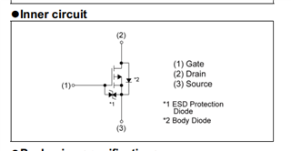
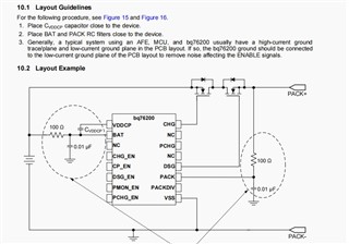
I have attached schematic as well as a MOSFET data sheet for your reference.
We are using 2 Mosfets in parallel. (Vds = 100V, Vgs= +/ - 20V, Vgsth= 2 to 4V Ciss = 15000pf, )
Everything is working fine with a discharge current of 70A. However, discharge MOSFET is getting short during direct load short circuit test.
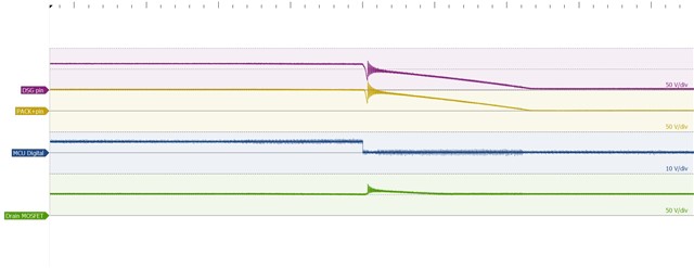
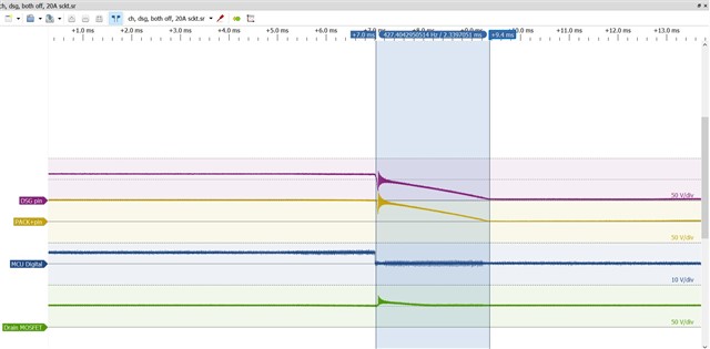
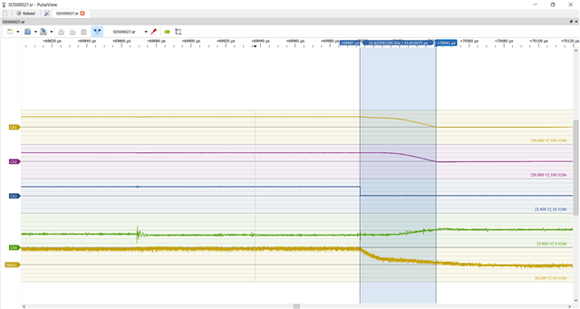
We tried to capture the waveform during a 40A short circuit test. Here MOSFET is not failing but we are observing some ringing oscillations at Source and gate of Discharge Mosfet which might be the reason behind MOSFET damage during Load short circuit.
As per Datasheet and application notes , turn off is carried out in 2 phases.
1. 1st phase - DSG pin is pull down to Source(PACK+) voltage With RC time contact depending upon Rdsg resistor. ( For our circuit, 12 uS - is happening within 22uS as per waveforms captured on oscilloscope)
Rdsg is 200 ohm with seperate ferrite bead for each MOSFET. I tried changing Rdsg but it had no effect on oscillation, only the initial delay is changing.
2. Dsg pin and Pack+ fall down to 0/Pack- - During this period there are some oscillations on DSG pin and PACK+ . DSG is following PACK+ . This period is getting delayed. PACK= is falling down to 0 after 4mS. We doubt this is preventing the MOSFET from turn off and current is still flowing.
( Oscilloscope waveforms are attached during 40A short circuit test)
Some more Observations:
1.No effect on Charge MOSFET
2. Either Discharge MOSFET is getting damaged.
3. Tried changing Rdsg value (R29 in schamatic form 100 ohm to 1K, no effect on oscillations)
4. Tried adding snubber circuit (No effect)
5. Tried changing Rgs value from 10 M to 20 M , no effect.
I request your support in reviewing the design and debugging this issue.
Please let me know if any change is required.
Waiting for your reply.
Thanks & regards,