


Hi WV team,
I am looking at the datasheet of TPSM365R15 and I have some question regarding the minimum input voltage.
I am assuming an application where Vin is not stable and falls down to 0V from high voltage.
First, the Vin falling minimum typical value is set at 3.0V.
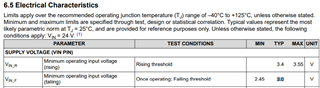
Additionally VCC is also 3.65, worst case.
So, when VCC is taken from Vin, the min Vin should be set 3.65V, worst case. Am I correct on this?
Secondly, this IC seems to have special feature "7.4.3.5 Dropout", where even when the Vin is below Vout, it will try to follow the Vin value, described by the below picture.
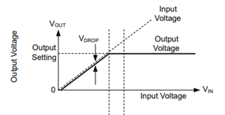
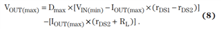
1. Assuming we are operating above minimum Vin, for example, 20V and creeping down to 5V, where set voltage Vout=10V. How should one can calculate the VDROP described in this picture. My understanding is that at this point the DCDC operates at max duty cycle 98%, Rds on for HS and LS, series inductance should be playing a role, but it is not mentioned in this section. Can you help me here?
FYI, I am referencing basic DCDC topology described in this old apps note. https://www.ti.com/lit/an/slyt293/slyt293.pdf?ts=1713319693943&ref_url=https%253A%252F%252Fwww.google.com%252F
2. With minimum Vin being 3V even with external VCC, shouldnt the X-axis cut-off on the left side? It seems like Vout will follow the Vin to 0V. I think it will "shut down" at some point.
Frankly speaking, i am trying to calculate this shut down cut voltage, but it is related to above question.
Thanks,
Luke

