This thread has been locked.

If you have a related question, please click the "Ask a related question" button in the top right corner. The newly created question will be automatically linked to this question.

BQ76952: I2C communication issue with BQ7695202 with STM MCU

Part Number: BQ76952
Other Parts Discussed in Thread: BQSTUDIO, EV2400,

Dear Team,

Our team has developed a custom hardware circuit employing the BQ7695202, with communication facilitated through the STM32L433 MCU via I2C.

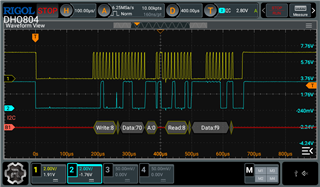
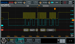
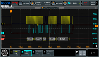
Regrettably, we are encountering difficulties in reading information from or establishing communication between the BQ7695202 and the MCU.

We kindly request your support in diagnosing the issue and providing recommendations for resolution.

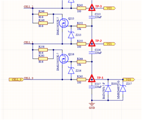
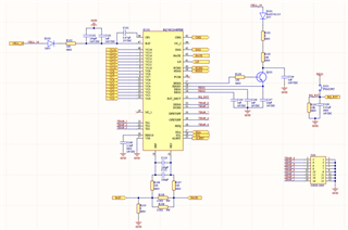
Enclosed is a segment of the schematic for your reference below

We have 4.7k Pull resistor on SDA and SCL

On hardware we are getting REG18 - 1.8V , REG1 - 3.4V and REG2 - 0V

Please suggest is there any other parameter we can test on hardware?

I'm also sharing our STM C file for reference

Also,

When we use 'HAL_I2C_IsDeviceReady' lib function to check device ready, it returns HAL_ERROR

/* USER CODE BEGIN Header */
/**
 ******************************************************************************
 * @file           : main.c
 * @brief          : Main program body
 ******************************************************************************
 * @attention
 *
 * Copyright (c) 2024 STMicroelectronics.
 * All rights reserved.
 *
 * This software is licensed under terms that can be found in the LICENSE file
 * in the root directory of this software component.
 * If no LICENSE file comes with this software, it is provided AS-IS.
 *
 ******************************************************************************
 */
/* USER CODE END Header */
/* Includes ------------------------------------------------------------------*/
#include "main.h"
#include "adc.h"
#include "dma.h"
#include "i2c.h"
#include "tim.h"
#include "usart.h"
#include "gpio.h"

/* Private includes ----------------------------------------------------------*/
/* USER CODE BEGIN Includes */
#include "BQ769x2Header.h"
#include "stdio.h"
/* USER CODE END Includes */

/* Private typedef -----------------------------------------------------------*/
/* USER CODE BEGIN PTD */

/* USER CODE END PTD */

/* Private define ------------------------------------------------------------*/
/* USER CODE BEGIN PD */
#define DEV_ADDR  0x10  // BQ769x2 address is 0x10 including R/W bit or 0x8 as 7-bit address
#define CRC_Mode 0  // 0 for disabled, 1 for enabled
#define MAX_BUFFER_SIZE     10
/* USER CODE END PD */

/* Private macro -------------------------------------------------------------*/
/* USER CODE BEGIN PM */

/* USER CODE END PM */

/* Private variables ---------------------------------------------------------*/

/* USER CODE BEGIN PV */
uint8_t spiData[2];
uint8_t spiRxData[2];
uint8_t rxdata[2];
uint8_t busyData[2] = { 0xFF, 0xFF };

uint8_t TX_2Byte[2] = { 0x00, 0x00 };
uint8_t TX_3Byte[3] = { 0x00, 0x00, 0x00 };
uint8_t TX_4Byte[4] = { 0x00, 0x00, 0x00, 0x00 };
uint8_t TX_Buffer[MAX_BUFFER_SIZE] = { 0x00, 0x00, 0x00, 0x00, 0x00, 0x00, 0x00,
		0x00, 0x00, 0x00 };

uint8_t RX_2Byte[2] = { 0x00, 0x00 };
uint8_t RX_3Byte[3] = { 0x00, 0x00, 0x00 };
uint8_t RX_4Byte[4] = { 0x00, 0x00, 0x00, 0x00 };
uint8_t RX_12Byte[12] = { 0x00, 0x00, 0x00, 0x00, 0x00, 0x00, 0x00, 0x00, 0x00,
		0x00, 0x00, 0x00 };
uint8_t RX_Buffer[MAX_BUFFER_SIZE] = { 0x00, 0x00, 0x00, 0x00, 0x00, 0x00, 0x00,
		0x00, 0x00, 0x00 };
unsigned int RX_CRC_Check = 0;

// Variables for cell voltages, temperatures, CC2 current, Stack voltage, PACK Pin voltage, LD Pin voltage
uint16_t CellVoltage[16] = { 0x00, 0x00, 0x00, 0x00, 0x00, 0x00, 0x00, 0x00,
		0x00, 0x00, 0x00, 0x00, 0x00, 0x00, 0x00, 0x00 };
float Temperature[3] = { 0, 0, 0 };
float FET_Temperature = 0;
uint16_t Stack_Voltage = 0x00;
uint16_t LD_Voltage = 0x00;
uint16_t PACK_Voltage = 0x00;
uint16_t PACK_Current = 0x00;
uint16_t AlarmBits = 0x00;

uint8_t SafetyStatusA; // Safety Status Register A
uint8_t SafetyStatusB; // Safety Status Register B
uint8_t SafetyStatusC; // Safety Status Register C
uint8_t PFStatusA; // Permanent Fail Status Register A
uint8_t PFStatusB; // Permanent Fail Status Register B
uint8_t PFStatusC; // Permanent Fail Status Register C
uint8_t FET_Status; // FET Status register contents See TRM Section 12.2.20  - Shows states of FETs

uint16_t CB_ActiveCells;  // Cell Balancing Active Cells
uint16_t DEVICE_NUMBER;

uint8_t UV_Fault = 0;   // under-voltage fault state
uint8_t OV_Fault = 0;   // over-voltage fault state
uint8_t SCD_Fault = 0;  // short-circuit fault state
uint8_t OCD_Fault = 0;  // over-current fault state
uint8_t LD_ON = 0;							// Load Detect status bit
uint8_t DCHG = 0;   // discharge FET state
uint8_t CHG = 0;   // charge FET state
uint8_t PCHG = 0;  // pre-charge FET state
uint8_t PDSG = 0;  // pre-discharge FET state

uint32_t AccumulatedCharge_Int;
uint32_t AccumulatedCharge_Frac;
uint32_t AccumulatedCharge_Time;
/* USER CODE END PV */

/* Private function prototypes -----------------------------------------------*/
void SystemClock_Config(void);
/* USER CODE BEGIN PFP */

void CopyArray(uint8_t *source, uint8_t *dest, uint8_t count) {
	uint8_t copyIndex = 0;
	for (copyIndex = 0; copyIndex < count; copyIndex++) {
		dest[copyIndex] = source[copyIndex];
	}
}

unsigned char Checksum(unsigned char *ptr, unsigned char len)
// Calculates the checksum when writing to a RAM register. The checksum is the inverse of the sum of the bytes.
{
	unsigned char i;
	unsigned char checksum = 0;

	for (i = 0; i < len; i++)
		checksum += ptr[i];

	checksum = 0xff & ~checksum;

	return (checksum);
}

unsigned char CRC8(unsigned char *ptr, unsigned char len) {
	unsigned char i;
	unsigned char crc = 0;
	while (len-- != 0) {
		for (i = 0x80; i != 0; i /= 2) {
			if ((crc & 0x80) != 0) {
				crc *= 2;
				crc ^= 0x107;
			} else
				crc *= 2;

			if ((*ptr & i) != 0)
				crc ^= 0x107;
		}
		ptr++;
	}
	return (crc);
}

void I2C_WriteReg(uint8_t reg_addr, uint8_t *reg_data, uint8_t count) {
#if CRC_Mode
		{
		uint8_t crc_count = 0;
		crc_count = count * 2;
		uint8_t crc1stByteBuffer [3] = {0x10, reg_addr, reg_data[0]};
		unsigned int j;
		unsigned int i;
		uint8_t temp_crc_buffer [3];

		TX_Buffer[0] = reg_data[0];
		TX_Buffer[1] = CRC8(crc1stByteBuffer,3);

		j = 2;
		for(i=1; i<count; i++)
		{
			TX_Buffer[j] = reg_data[i];
			j = j + 1;
			temp_crc_buffer[0] = reg_data[i];
			TX_Buffer[j] = CRC8(temp_crc_buffer,1);
			j = j + 1;
		}
		HAL_I2C_Mem_Write(&hi2c1, DEV_ADDR, reg_addr, 1, TX_Buffer, count, 1000);
		}
		#endif

#if CRC_Mode < 1
	// HAL_I2C_Mem_Write(&hi2c1, DEV_ADDR, reg_addr, 1, reg_data, count, 1000);
	HAL_I2C_Mem_Write_DMA(&hi2c1, DEV_ADDR, reg_addr, 1, reg_data, count);
#endif
}

int I2C_ReadReg(uint8_t reg_addr, uint8_t *reg_data, uint8_t count) {
	unsigned int RX_CRC_Fail = 0; // reset to 0. If in CRC Mode and CRC fails, this will be incremented.

#if CRC_Mode
	{
		uint8_t crc_count = 0;
		uint8_t ReceiveBuffer [10] = {0x00,0x00,0x00,0x00,0x00,0x00,0x00,0x00,0x00,0x00};
		crc_count = count * 2;
		unsigned int j;
		unsigned int i;
		unsigned char CRCc = 0;
		uint8_t temp_crc_buffer [3];

		HAL_I2C_Mem_Read(&hi2c1, DEV_ADDR, reg_addr, 1, ReceiveBuffer, crc_count, 1000);
		uint8_t crc1stByteBuffer [4] = {0x10, reg_addr, 0x11, ReceiveBuffer[0]};
		CRCc = CRC8(crc1stByteBuffer,4);
		if (CRCc != ReceiveBuffer[1])
			RX_CRC_Fail += 1;

		RX_Buffer[0] = ReceiveBuffer[0];

		j = 2;
		for (i=1; i<count; i++)
		{
			RX_Buffer[i] = ReceiveBuffer[j];
			temp_crc_buffer[0] = ReceiveBuffer[j];
			j = j + 1;
			CRCc = CRC8(temp_crc_buffer,1);
			if (CRCc != ReceiveBuffer[j])
				RX_CRC_Fail += 1;
			j = j + 1;
		}
		CopyArray(RX_Buffer, reg_data, crc_count);
	}
	#endif

#if CRC_Mode < 1
	// HAL_I2C_Mem_Read(&hi2c1, DEV_ADDR, reg_addr, 1, reg_data, count, 1000);
	HAL_I2C_Mem_Read_DMA(&hi2c1, DEV_ADDR, reg_addr, 1, reg_data, count);
#endif

	return 0;
}

void AFE_Reset() {
	// Reset command. Resets all registers to default values or the values programmed in OTP.
	TX_2Byte[0] = 0x12;
	TX_2Byte[1] = 0x00;
	I2C_WriteReg(0x3E, TX_2Byte, 2);
}

void AFE_Init() {
	// Configures all parameters in device RAM

	// Enter CONFIGUPDATE mode (Subcommand 0x0090) - It is required to be in CONFIG_UPDATE mode to program the device RAM settings
	// See TRM Section 7.6 for full description of CONFIG_UPDATE mode
	TX_2Byte[0] = 0x90;
	TX_2Byte[1] = 0x00;
	I2C_WriteReg(0x3E, TX_2Byte, 2);

	//  delayUS(2000);

	// After entering CONFIG_UPDATE mode, RAM registers can be programmed. When programming RAM, checksum and length must also be
	// programmed for the change to take effect. All of the RAM registers are described in detail in Chapter 13 of the BQ76952 TRM.
	// An easier way to find the descriptions is in the BQStudio Data Memory screen. When you move the mouse over the register name,
	// a full description of the register and the bits will pop up on the screen.
	// A summary of the Data Memory is also in Section 13.9 of the TRM.

	// 'Power Config' - Set DSLP_LDO  - 0x9234 = 0x2D82  (See TRM section 13.3.2)
	// Setting the DSLP_LDO bit allows the LDOs to remain active when the device goes into Deep Sleep mode
	TX_4Byte[0] = 0x34;
	TX_4Byte[1] = 0x92;
	TX_4Byte[2] = 0x82;
	TX_4Byte[3] = 0x2D;
	I2C_WriteReg(0x3E, TX_4Byte, 4);
	//  delayUS(1000);
	TX_2Byte[0] = Checksum(TX_4Byte, 4);
	TX_2Byte[1] = 0x06;  // Checksum and Length
	I2C_WriteReg(0x60, TX_2Byte, 2);
	//  delayUS(1000);

	// 'REG0 Config' - set REG0_EN bit to enable pre-regulator
	TX_3Byte[0] = 0x37;
	TX_3Byte[1] = 0x92;
	TX_3Byte[2] = 0x01;
	I2C_WriteReg(0x3E, TX_3Byte, 3);
	//  delayUS(1000);
	TX_2Byte[0] = Checksum(TX_3Byte, 3);
	TX_2Byte[1] = 0x05;
	I2C_WriteReg(0x60, TX_2Byte, 2);
	//  delayUS(1000);

	// 'REG12 Config' - Enable REG1 with 3.3V output
	TX_3Byte[0] = 0x36;
	TX_3Byte[1] = 0x92;
	TX_3Byte[2] = 0x0D;
	I2C_WriteReg(0x3E, TX_3Byte, 3);
	//  delayUS(1000);
	TX_2Byte[0] = Checksum(TX_3Byte, 3);
	TX_2Byte[1] = 0x05;
	I2C_WriteReg(0x60, TX_2Byte, 2);
	//  delayUS(1000);

	// 'VCell Mode' - Enable 16 cells - 0x9304 = 0x0000  (See TRM section 13.3.2.19)
	// 0x0000 sets the default value of 16 cells.
	TX_4Byte[0] = 0x04;
	TX_4Byte[1] = 0x93;
	TX_4Byte[2] = 0x00;
	TX_4Byte[3] = 0x00;
	I2C_WriteReg(0x3E, TX_4Byte, 4);
	//  delayUS(1000);
	TX_2Byte[0] = Checksum(TX_4Byte, 4);
	TX_2Byte[1] = 0x06;  // Checksum and Length
	I2C_WriteReg(0x60, TX_2Byte, 2);
	//  delayUS(1000);

	// 'Default Alarm Mask' - Enable FullScan and ADScan bits
	// 0xF882
	TX_4Byte[0] = 0x6D;
	TX_4Byte[1] = 0x92;
	TX_4Byte[2] = 0x82;
	TX_4Byte[3] = 0xF8;
	I2C_WriteReg(0x3E, TX_4Byte, 4);
	//  delayUS(1000);
	TX_2Byte[0] = Checksum(TX_4Byte, 4);
	TX_2Byte[1] = 0x06;  // Checksum and Length
	I2C_WriteReg(0x60, TX_2Byte, 2);
	//  delayUS(1000);

	// Enable protections in 'Enabled Protections A' 0x9261 = 0xBC (See TRM section 13.3.3.2)
	// Enables SCD (short-circuit), OCD1 (over-current in discharge), OCC (over-current in charge),
	// COV (over-voltage), CUV (under-voltage)
	TX_3Byte[0] = 0x61;
	TX_3Byte[1] = 0x92;
	TX_3Byte[2] = 0xFC;
	I2C_WriteReg(0x3E, TX_3Byte, 3);
	//  delayUS(1000);
	TX_2Byte[0] = Checksum(TX_3Byte, 3);
	TX_2Byte[1] = 0x05;
	I2C_WriteReg(0x60, TX_2Byte, 2);
	//  delayUS(1000);

	// Enable all protections in 'Enabled Protections B' 0x9262 = 0xF7 (See TRM section 13.3.3.3)
	// Enables OTF (over-temperature FET), OTINT (internal over-temperature), OTD (over-temperature in discharge),
	// OTC (over-temperature in charge), UTINT (internal under-temperature), UTD (under-temperature in discharge), UTC (under-temperature in charge)
	TX_3Byte[0] = 0x62;
	TX_3Byte[1] = 0x92;
	TX_3Byte[2] = 0xF7;
	I2C_WriteReg(0x3E, TX_3Byte, 3);
	//  delayUS(1000);
	TX_2Byte[0] = Checksum(TX_3Byte, 3);
	TX_2Byte[1] = 0x05;
	I2C_WriteReg(0x60, TX_2Byte, 2);
	//  delayUS(1000);

	// Set TS1 to measure Cell Temperature - 0x92FD = 0x07   (See TRM Section 13.3.2.12)
	TX_3Byte[0] = 0xFD;
	TX_3Byte[1] = 0x92;
	TX_3Byte[2] = 0x07;
	I2C_WriteReg(0x3E, TX_3Byte, 3);
	//  delayUS(1000);
	TX_2Byte[0] = Checksum(TX_3Byte, 3);
	TX_2Byte[1] = 0x05;
	I2C_WriteReg(0x60, TX_2Byte, 2);
	//  delayUS(1000);

	// Set TS3 to measure FET Temperature - 0x92FF = 0x0F   (See TRM Section 13.3.2.14)
	TX_3Byte[0] = 0xFF;
	TX_3Byte[1] = 0x92;
	TX_3Byte[2] = 0x0F;
	I2C_WriteReg(0x3E, TX_3Byte, 3);
	//  delayUS(1000);
	TX_2Byte[0] = Checksum(TX_3Byte, 3);
	TX_2Byte[1] = 0x05;
	I2C_WriteReg(0x60, TX_2Byte, 2);
	//  delayUS(1000);

	// Set DFETOFF pin to control BOTH CHG and DSG FET - 0x92FB = 0x42 (set to 0x00 to disable)
	// See TRM section 13.3.2.10, Table 13-7
	TX_3Byte[0] = 0xFB;
	TX_3Byte[1] = 0x92;
	TX_3Byte[2] = 0x42;
	I2C_WriteReg(0x3E, TX_3Byte, 3);
	//  delayUS(1000);
	TX_2Byte[0] = Checksum(TX_3Byte, 3);
	TX_2Byte[1] = 0x05;
	I2C_WriteReg(0x60, TX_2Byte, 2);
	//  delayUS(1000);

	// Set up Alert Pin - 0x92FC = 0x2A  - See TRM Section 13.3.2.11, Table 13-8
	// This configures the Alert pin to drive high (REG1 voltage) when enabled.
	// Other options available include active-low, drive HiZ, drive using REG18 (1.8V), weak internal pull-up and pull-down
	TX_3Byte[0] = 0xFC;
	TX_3Byte[1] = 0x92;
	TX_3Byte[2] = 0x2A;
	I2C_WriteReg(0x3E, TX_3Byte, 3);
	//  delayUS(1000);
	TX_2Byte[0] = Checksum(TX_3Byte, 3);
	TX_2Byte[1] = 0x05;
	I2C_WriteReg(0x60, TX_2Byte, 2);
	//  delayUS(1000);

	// Set up Cell Balancing Configuration - 0x9335 = 0x03   -  Automated balancing while in Relax or Charge modes
	// See TRM Section 13.3.11. Chapter 10 of TRM describes Cell Balancing in detail
	// Also see "Cell Balancing with BQ76952, BQ76942 Battery Monitors" document on ti.com
	TX_3Byte[0] = 0x35;
	TX_3Byte[1] = 0x93;
	TX_3Byte[2] = 0x03;
	I2C_WriteReg(0x3E, TX_3Byte, 3);
	//  delayUS(1000);
	TX_2Byte[0] = Checksum(TX_3Byte, 3);
	TX_2Byte[1] = 0x05;
	I2C_WriteReg(0x60, TX_2Byte, 2);
	//  delayUS(1000);

	// Set up COV (over-voltage) Threshold - 0x9278 = 0x55 (4301 mV)
	// COV Threshold is this value multiplied by 50.6mV  See TRM section 13.6.2
	TX_3Byte[0] = 0x78;
	TX_3Byte[1] = 0x92;
	TX_3Byte[2] = 0x55;
	I2C_WriteReg(0x3E, TX_3Byte, 3);
	//  delayUS(1000);
	TX_2Byte[0] = Checksum(TX_3Byte, 3);
	TX_2Byte[1] = 0x05;
	I2C_WriteReg(0x60, TX_2Byte, 2);
	//  delayUS(1000);

	// Set up SCD Threshold - 0x9286 = 0x05 (100 mV = 100A across 1mOhm sense resistor)
	// See TRM section 13.6.7    0x05=100mV
	TX_3Byte[0] = 0x86;
	TX_3Byte[1] = 0x92;
	TX_3Byte[2] = 0x05;
	I2C_WriteReg(0x3E, TX_3Byte, 3);
	//  delayUS(1000);
	TX_2Byte[0] = Checksum(TX_3Byte, 3);
	TX_2Byte[1] = 0x05;
	I2C_WriteReg(0x60, TX_2Byte, 2);
	//  delayUS(1000);

	// Set up SCD Delay - 0x9287 = 0x03 (30 us)    See TRM section 13.6.7
	// Units of 15us
	TX_3Byte[0] = 0x87;
	TX_3Byte[1] = 0x92;
	TX_3Byte[2] = 0x03;
	I2C_WriteReg(0x3E, TX_3Byte, 3);
	//  delayUS(1000);
	TX_2Byte[0] = Checksum(TX_3Byte, 3);
	TX_2Byte[1] = 0x05;
	I2C_WriteReg(0x60, TX_2Byte, 2);
	//  delayUS(1000);

	// Set up SCDL Latch Limit to 1 to set SCD recovery only with load removal 0x9295 = 0x01
	// If this is not set, then SCD will recover based on time (SCD Recovery Time parameter).
	// See TRM section 13.6.11.1
	TX_3Byte[0] = 0x95;
	TX_3Byte[1] = 0x92;
	TX_3Byte[2] = 0x01;
	I2C_WriteReg(0x3E, TX_3Byte, 3);
	//  delayUS(1000);
	TX_2Byte[0] = Checksum(TX_3Byte, 3);
	TX_2Byte[1] = 0x05;
	I2C_WriteReg(0x60, TX_2Byte, 2);
	//  delayUS(1000);

	// Exit CONFIGUPDATE mode  - Subcommand 0x0092
	TX_2Byte[0] = 0x92;
	TX_2Byte[1] = 0x00;
	I2C_WriteReg(0x3E, TX_2Byte, 2);
	//  delayUS(1000);
}

//  ********************************* FET Control Commands  ***************************************

void AFE_FET_ENABLE() {
	// Toggles the FET_EN bit in the Manufacturing Status register. So this command can be used to enable or disable the FETs.
	TX_2Byte[0] = 0x22;
	TX_2Byte[1] = 0x00;
	I2C_WriteReg(0x3E, TX_2Byte, 2);
}

void AFE_FET_Control(uint8_t FET_states) { // Bit3 = PCHG_OFF, Bit 2 = CHG_OFF, Bit1 = PDSG_OFF, Bit 0 = DSG_OFF
	TX_3Byte[0] = 0x97;
	TX_3Byte[1] = 0x00;
	TX_3Byte[2] = FET_states;
	I2C_WriteReg(0x3E, TX_3Byte, 3);
	//  delayUS(1000);
	TX_2Byte[0] = Checksum(TX_3Byte, 3);
	TX_2Byte[1] = 0x05;
	I2C_WriteReg(0x60, TX_2Byte, 2);
}

void DSG_PDSG_OFF() {
	// Disable discharge (and pre-discharge) FETs
	// Subcommand 0x0093  See TRM Table 5-8  (DSG_PDSG_OFF())
	TX_2Byte[0] = 0x93;
	TX_2Byte[1] = 0x00;
	I2C_WriteReg(0x3E, TX_2Byte, 2);
}

void CHG_PCHG_OFF() {
	// Disable charge (and pre-charge) FETs
	// Subcommand 0x0094  See TRM Table 5-8  (CHG_PCHG_OFF())
	TX_2Byte[0] = 0x94;
	TX_2Byte[1] = 0x00;
	I2C_WriteReg(0x3E, TX_2Byte, 2);
}

void AFE_ALL_FETS_OFF() {
	// Disable all FETs with command 0x0095  See TRM Table 5-8
	TX_2Byte[0] = 0x95;
	TX_2Byte[1] = 0x00;
	I2C_WriteReg(0x3E, TX_2Byte, 2);
}

void AFE_ALL_FETS_ON() {
	// All all FETs to be enabled with command 0x0096  See TRM Table 5-8
	TX_2Byte[0] = 0x96;
	TX_2Byte[1] = 0x00;
	I2C_WriteReg(0x3E, TX_2Byte, 2);
}

void AFE_BOTHOFF() {
	// Disables all FETs using the DFETOFF (BOTHOFF) pin
	HAL_GPIO_WritePin(DFETOFF_GPIO_Port, DFETOFF_Pin, GPIO_PIN_SET); // DFETOFF pin (BOTHOFF) set high

}

void AFE_RESET_BOTHOFF() {
	// Resets DFETOFF (BOTHOFF) pin
	HAL_GPIO_WritePin(DFETOFF_GPIO_Port, DFETOFF_Pin, GPIO_PIN_RESET); // DFETOFF pin (BOTHOFF) set low
}

void AFE_ReadFETStatus() {
	// Read FET Status to see which FETs are enabled
	I2C_ReadReg(0x7F, RX_2Byte, 2);
	FET_Status = (RX_2Byte[1] * 256 + RX_2Byte[0]);
	DCHG = 0x4 & RX_2Byte[0];   // discharge FET state
	CHG = 0x1 & RX_2Byte[0];   // charge FET state
	PCHG = 0x2 & RX_2Byte[0];  // pre-charge FET state
	PDSG = 0x8 & RX_2Byte[0];  // pre-discharge FET state
}

// ********************************* End of FET Control Commands *********************************

// ********************************* AFE Cell Balancing Commands   *****************************************

void CB_ACTIVE_CELLS() {
	// Check status of which cells are balancing
	TX_2Byte[0] = 0x83;
	TX_2Byte[1] = 0x00;
	I2C_WriteReg(0x3E, TX_2Byte, 2);
	I2C_ReadReg(0x40, RX_2Byte, 2);
	CB_ActiveCells = (RX_2Byte[1] * 256 + RX_2Byte[0]);
}

// ********************************* End of AFE Cell Balancing Commands   *****************************************

// ********************************* AFE Power Commands   *****************************************
void AFE_DeepSleep() {
	// Puts the device into DEEPSLEEP mode. See TRM section 7.4
	TX_2Byte[0] = 0x0F;
	TX_2Byte[1] = 0x00;
	I2C_WriteReg(0x3E, TX_2Byte, 2);
	I2C_WriteReg(0x3E, TX_2Byte, 2);
}

void AFE_ExitDeepSleep() {
	// Exits DEEPSLEEP mode. See TRM section 7.4
	TX_2Byte[0] = 0x0E;
	TX_2Byte[1] = 0x00;
	I2C_WriteReg(0x3E, TX_2Byte, 2);
}

void AFE_ShutdownCommand() {
	// Puts the device into SHUTDOWN mode. See TRM section 7.5
	TX_2Byte[0] = 0x10;
	TX_2Byte[1] = 0x00;
	I2C_WriteReg(0x3E, TX_2Byte, 2);
}

void AFE_ShutdownPin() {
	// Puts the device into SHUTDOWN mode using the RST_SHUT pin
	HAL_GPIO_WritePin(BQ_RST_GPIO_Port, BQ_RST_Pin, GPIO_PIN_SET); // Sets RST_SHUT pin
}

void AFE_ReleaseShutdownPin() {
	// Releases the RST_SHUT pin
	HAL_GPIO_WritePin(BQ_RST_GPIO_Port, BQ_RST_Pin, GPIO_PIN_RESET); // Resets RST_SHUT pin
}

void AFE_SLEEP_ENABLE() { // SLEEP_ENABLE 0x0099
	// Allows the device to enter Sleep mode if current is below Sleep Current. See TRM section 7.3
	TX_2Byte[0] = 0x99;
	TX_2Byte[1] = 0x00;
	I2C_WriteReg(0x3E, TX_2Byte, 2);
}

void AFE_SLEEP_DISABLE() { // SLEEP_DISABLE 0x009A
	// Takes the device out of sleep mode. See TRM section 7.3
	TX_2Byte[0] = 0x9A;
	TX_2Byte[1] = 0x00;
	I2C_WriteReg(0x3E, TX_2Byte, 2);
}

// ********************************* End of AFE Power Commands   *****************************************

// ********************************* AFE Status and Fault Commands   *****************************************

uint16_t AFE_ReadAlarmStatus() {
	// Read this register to find out why the Alert pin was asserted. See section 6.6 of the TRM for full description.
	I2C_ReadReg(0x62, RX_2Byte, 2);
	return (RX_2Byte[1] * 256 + RX_2Byte[0]);
}

void AFE_ReadSafetyStatus() {
	// Read Safety Status A/B/C and find which bits are set
	// This shows which primary protections have been triggered
	I2C_ReadReg(0x03, RX_2Byte, 2);
	SafetyStatusA = (RX_2Byte[1] * 256 + RX_2Byte[0]);
	UV_Fault = 0x4 & RX_2Byte[0];
	OV_Fault = 0x8 & RX_2Byte[0];
	SCD_Fault = 0x8 & RX_2Byte[1];
	OCD_Fault = 0x2 & RX_2Byte[1];
	I2C_ReadReg(0x05, RX_2Byte, 2);
	SafetyStatusB = (RX_2Byte[1] * 256 + RX_2Byte[0]);
	I2C_ReadReg(0x07, RX_2Byte, 2);
	SafetyStatusC = (RX_2Byte[1] * 256 + RX_2Byte[0]);
}

void AFE_ReadPFStatus() {
	// Read Permanent Fail Status A/B/C and find which bits are set
	// This shows which permanent failures have been triggered
	I2C_ReadReg(0x0B, RX_2Byte, 2);
	PFStatusA = (RX_2Byte[1] * 256 + RX_2Byte[0]);
	I2C_ReadReg(0x0D, RX_2Byte, 2);
	PFStatusB = (RX_2Byte[1] * 256 + RX_2Byte[0]);
	I2C_ReadReg(0x0F, RX_2Byte, 2);
	PFStatusC = (RX_2Byte[1] * 256 + RX_2Byte[0]);
}

void AFE_ControlStatus() {
	// Control status register - Bit0 - LD_ON (load detected)
	// See TRM Table 6-1
	I2C_ReadReg(0x00, RX_2Byte, 2);
	LD_ON = 0x1 & RX_2Byte[0];
}

void AFE_BatteryStatus() {
	// Battery status register - See TRM Table 6-2
	I2C_ReadReg(0x12, RX_2Byte, 2);
}

void AFE_ClearFaults() {
	TX_2Byte[0] = 0x00;
	TX_2Byte[1] = 0xF8;
	I2C_WriteReg(0x62, TX_2Byte, 2);
}

void AFE_ClearScanBits() {
	TX_2Byte[0] = 0x82;
	TX_2Byte[1] = 0x00;
	I2C_WriteReg(0x62, TX_2Byte, 2);
}

void AFE_PFReset() {
	TX_2Byte[0] = 0x29;
	TX_2Byte[1] = 0x00;
	I2C_WriteReg(0x3E, TX_2Byte, 2);
}

uint16_t AFE_DeviceID() {
	// Read Device ID using Subcommand 0x0001
	TX_2Byte[0] = 0x01;
	TX_2Byte[1] = 0x00;
	I2C_WriteReg(0x3E, TX_2Byte, 2);
	//  delayUS(500);
	I2C_ReadReg(0x40, RX_2Byte, 2);
	return (RX_2Byte[1] * 256 + RX_2Byte[0]);
}
// ********************************* End of AFE Status and Fault Commands   *****************************************

// ********************************* AFE Measurement Commands   *****************************************

uint16_t AFE_ReadCellVoltage(uint8_t channel) {
	I2C_ReadReg(channel * 2 + 0x12, RX_2Byte, 2);
	return (RX_2Byte[1] * 256 + RX_2Byte[0]);  // cell voltage is reported in mV
}

uint16_t AFE_ReadStackVoltage() {
	I2C_ReadReg(0x34, RX_2Byte, 2);
	return 10 * (RX_2Byte[1] * 256 + RX_2Byte[0]); // voltage is reported in 0.01V units
}

uint16_t AFE_ReadPackVoltage() {
	I2C_ReadReg(0x36, RX_2Byte, 2);
	return 10 * (RX_2Byte[1] * 256 + RX_2Byte[0]); // voltage is reported in 0.01V units
}

uint16_t AFE_ReadLDVoltage() {
	I2C_ReadReg(0x38, RX_2Byte, 2);
	return 10 * (RX_2Byte[1] * 256 + RX_2Byte[0]); // voltage is reported in 0.01V units
}

uint16_t AFE_ReadCurrent() {
	I2C_ReadReg(0x3A, RX_2Byte, 2);
	return (RX_2Byte[1] * 256 + RX_2Byte[0]);  // current is reported in mA
}

float AFE_ReadTemperature(uint8_t channel) {
	switch (channel) {
	case 0:
		I2C_ReadReg(0x70, RX_2Byte, 2);  // TS1 pin
		break;
	case 1:
		I2C_ReadReg(0x74, RX_2Byte, 2);  // TS3 pin, FET temperature
		break;
	default:
		break;
	}
	return (0.1 * (float) (RX_2Byte[1] * 256 + RX_2Byte[0])) - 273.15; // convert from 0.1K to Celcius
}

void AFE_ReadPassQ() {
	// Read Accumulated Charge and Time from DASTATUS6 (See TRM Table 4-6)
	TX_2Byte[0] = 0x76;
	TX_2Byte[1] = 0x00;
	I2C_WriteReg(0x3E, TX_2Byte, 2);
	//  delayUS(1000);
	I2C_ReadReg(0x40, RX_12Byte, 12);
	AccumulatedCharge_Int = ((RX_12Byte[3] << 24) + (RX_12Byte[2] << 16)
			+ (RX_12Byte[1] << 8) + RX_12Byte[0]);
	AccumulatedCharge_Frac = ((RX_12Byte[7] << 24) + (RX_12Byte[6] << 16)
			+ (RX_12Byte[5] << 8) + RX_12Byte[4]);
	AccumulatedCharge_Time = ((RX_12Byte[11] << 24) + (RX_12Byte[10] << 16)
			+ (RX_12Byte[9] << 8) + RX_12Byte[8]);
}

void AFE_ClearPassQ() {
	// Clear Accumulated Charge and Time, command 0x0082
	TX_2Byte[0] = 0x82;
	TX_2Byte[1] = 0x00;
	I2C_WriteReg(0x3E, TX_2Byte, 2);
}

/* USER CODE END PFP */

/* Private user code ---------------------------------------------------------*/
/* USER CODE BEGIN 0 */

/* USER CODE END 0 */

/**
 * @brief  The application entry point.
 * @retval int
 */
int main(void) {
	/* USER CODE BEGIN 1 */
	int i = 0;
	char uart_buf[50];
	int uart_buf_len;
	/* USER CODE END 1 */

	/* MCU Configuration--------------------------------------------------------*/

	/* Reset of all peripherals, Initializes the Flash interface and the Systick. */
	HAL_Init();

	/* USER CODE BEGIN Init */

	/* USER CODE END Init */

	/* Configure the system clock */
	SystemClock_Config();

	/* USER CODE BEGIN SysInit */

	/* USER CODE END SysInit */

	/* Initialize all configured peripherals */
	MX_GPIO_Init();
	MX_DMA_Init();
	MX_I2C1_Init();
	MX_USART3_UART_Init();
	MX_TIM1_Init();
	MX_ADC1_Init();
	MX_USART2_UART_Init();
	/* USER CODE BEGIN 2 */

	HAL_TIM_Base_Start(&htim1);
	printf("============Start Application===========\n");

//	uint8_t RxData1[2] = { 0x00, 0x00 };
//	uint8_t TxData1[2] = { 0x00, 0x00 };
	int ret = 0;
//
////	HAL_I2C_IsDeviceReady();
//
//	TxData1[0] = 0x82;
//	TxData1[1] = 0xF0;
//
//	ret = HAL_I2C_Mem_Read_DMA(&hi2c1, DEV_ADDR, 0x68, sizeof(uint16_t),
//			&RxData1[0], sizeof(uint16_t));
//	uint16_t Data = (RxData1[1] * 256 + RxData1[0]);
//	printf("Byte_1 - %x | Byte_2 - %x | ret - %d | Data - %d\n", RxData1[0],
//			RxData1[1], ret, Data);

//	uint8_t RxData[10];
//	int cellvoltageholder = Cell1Voltage; //Cell1Voltage is 0x14
//	for (int i = 1; i < 17; i++) {
//
//		HAL_I2C_Mem_Read_DMA(&hi2c1, DEV_ADDR, cellvoltageholder, 1, &RxData[0], 1);
//		printf("Cell-%d | ", i);
//		printf("Byte_1 - %x,  Byte_2 - %x \n", RxData[0], RxData[1]);
//		cellvoltageholder = cellvoltageholder + 2;
//	}

//	HAL_GPIO_WritePin(GPIOA, GPIO_PIN_9, GPIO_PIN_RESET); // RST_SHUT pin set low
//	HAL_GPIO_WritePin(GPIOA, GPIO_PIN_8, GPIO_PIN_RESET); // DFETOFF pin (BOTHOFF) set low
	HAL_GPIO_WritePin(BQ_RST_GPIO_Port, BQ_RST_Pin, GPIO_PIN_RESET); // RST_SHUT pin set low
	HAL_GPIO_WritePin(DFETOFF_GPIO_Port, DFETOFF_Pin, GPIO_PIN_RESET); // DFETOFF pin (BOTHOFF) set low
	HAL_Delay(1000);

	ret = HAL_I2C_IsDeviceReady(&hi2c1, DEV_ADDR, 1, 1000);
	HAL_Delay(1000);
	printf("Device Ready state - %d\n", ret);

	AFE_Reset();
	HAL_Delay(1000);
	//  delayUS(60000);
	AFE_Init();
	HAL_Delay(1000);
	//  delayUS(10000);
	AFE_FET_ENABLE();
	HAL_Delay(1000);
	//  delayUS(10000);

	AFE_SLEEP_DISABLE();
	HAL_Delay(1000);

//	ret = HAL_I2C_IsDeviceReady(&hi2c1, DEV_ADDR,1, 1000);
//	HAL_Delay(1000);
//	printf("Device Ready state - %d\n", ret);

	//  delayUS(60000); //  delayUS(60000); //  delayUS(60000); //  delayUS(60000);  //wait to start measurements after FETs close
	CellVoltage[1] = AFE_ReadCellVoltage(1);
	CellVoltage[5] = AFE_ReadCellVoltage(5);
	CellVoltage[10] = AFE_ReadCellVoltage(10);
	Stack_Voltage = AFE_ReadStackVoltage();
	PACK_Voltage = AFE_ReadPackVoltage();
	LD_Voltage = AFE_ReadLDVoltage();
	PACK_Current = AFE_ReadCurrent();
	Temperature[0] = AFE_ReadTemperature(0);
	FET_Temperature = AFE_ReadTemperature(1);

	/* USER CODE END 2 */

	/* Infinite loop */
	/* USER CODE BEGIN WHILE */
	while (1) {
		/* USER CODE END WHILE */

		/* USER CODE BEGIN 3 */
		CellVoltage[1] = AFE_ReadCellVoltage(1);

		//Debug code - prints the Cell1 Voltage to a terminal window
		uart_buf_len = sprintf(uart_buf, "%u mV\r\n", CellVoltage[1]);
		HAL_UART_Transmit(&huart2, (uint8_t*) uart_buf, uart_buf_len, 100);

		CellVoltage[2] = AFE_ReadCellVoltage(2);
		CellVoltage[3] = AFE_ReadCellVoltage(3);
		CellVoltage[4] = AFE_ReadCellVoltage(4);
		CellVoltage[5] = AFE_ReadCellVoltage(5);
		CellVoltage[6] = AFE_ReadCellVoltage(6);
		CellVoltage[7] = AFE_ReadCellVoltage(7);
		CellVoltage[8] = AFE_ReadCellVoltage(8);
		CellVoltage[9] = AFE_ReadCellVoltage(9);
		CellVoltage[10] = AFE_ReadCellVoltage(10);
		Stack_Voltage = AFE_ReadStackVoltage();
		PACK_Voltage = AFE_ReadPackVoltage();
		LD_Voltage = AFE_ReadLDVoltage();
		PACK_Current = AFE_ReadCurrent();
		Temperature[0] = AFE_ReadTemperature(0);
		FET_Temperature = AFE_ReadTemperature(1);

		AlarmBits = AFE_ReadAlarmStatus();
		//Debug code - prints the Cell1 Voltage to a terminal window
		uart_buf_len = sprintf(uart_buf, "%u \r\n", AlarmBits);
		HAL_UART_Transmit(&huart2, (uint8_t*) uart_buf, uart_buf_len, 100);

		if (AlarmBits & 0x82) {
			AFE_ClearScanBits();
		}

		if (AlarmBits & 0xC000) {
			AFE_ReadSafetyStatus();
			AFE_ReadPFStatus();
			AFE_ClearFaults();
			AFE_PFReset();
		}


	}
	/* USER CODE END 3 */
}

/**
 * @brief System Clock Configuration
 * @retval None
 */
void SystemClock_Config(void) {
	RCC_OscInitTypeDef RCC_OscInitStruct = { 0 };
	RCC_ClkInitTypeDef RCC_ClkInitStruct = { 0 };

	/** Configure the main internal regulator output voltage
	 */
	if (HAL_PWREx_ControlVoltageScaling(PWR_REGULATOR_VOLTAGE_SCALE1)
			!= HAL_OK) {
		Error_Handler();
	}

	/** Initializes the RCC Oscillators according to the specified parameters
	 * in the RCC_OscInitTypeDef structure.
	 */
	RCC_OscInitStruct.OscillatorType = RCC_OSCILLATORTYPE_HSI;
	RCC_OscInitStruct.HSIState = RCC_HSI_ON;
	RCC_OscInitStruct.HSICalibrationValue = RCC_HSICALIBRATION_DEFAULT;
	RCC_OscInitStruct.PLL.PLLState = RCC_PLL_ON;
	RCC_OscInitStruct.PLL.PLLSource = RCC_PLLSOURCE_HSI;
	RCC_OscInitStruct.PLL.PLLM = 1;
	RCC_OscInitStruct.PLL.PLLN = 10;
	RCC_OscInitStruct.PLL.PLLP = RCC_PLLP_DIV7;
	RCC_OscInitStruct.PLL.PLLQ = RCC_PLLQ_DIV2;
	RCC_OscInitStruct.PLL.PLLR = RCC_PLLR_DIV2;
	if (HAL_RCC_OscConfig(&RCC_OscInitStruct) != HAL_OK) {
		Error_Handler();
	}

	/** Initializes the CPU, AHB and APB buses clocks
	 */
	RCC_ClkInitStruct.ClockType = RCC_CLOCKTYPE_HCLK | RCC_CLOCKTYPE_SYSCLK
			| RCC_CLOCKTYPE_PCLK1 | RCC_CLOCKTYPE_PCLK2;
	RCC_ClkInitStruct.SYSCLKSource = RCC_SYSCLKSOURCE_PLLCLK;
	RCC_ClkInitStruct.AHBCLKDivider = RCC_SYSCLK_DIV1;
	RCC_ClkInitStruct.APB1CLKDivider = RCC_HCLK_DIV1;
	RCC_ClkInitStruct.APB2CLKDivider = RCC_HCLK_DIV1;

	if (HAL_RCC_ClockConfig(&RCC_ClkInitStruct, FLASH_LATENCY_4) != HAL_OK) {
		Error_Handler();
	}
}

/* USER CODE BEGIN 4 */
int _write(int file, char *ptr, int len) {
	for (int idx = 0; idx < len; idx++) {
		while (!(USART3->ISR & USART_ISR_TXE))
			;
		USART3->TDR = (uint8_t) ptr[idx];
	}

	return len;
}
/* USER CODE END 4 */

/**
 * @brief  This function is executed in case of error occurrence.
 * @retval None
 */
void Error_Handler(void) {
	/* USER CODE BEGIN Error_Handler_Debug */
	/* User can add his own implementation to report the HAL error return state */
	__disable_irq();
	while (1) {
	}
	/* USER CODE END Error_Handler_Debug */
}

#ifdef  USE_FULL_ASSERT
/**
  * @brief  Reports the name of the source file and the source line number
  *         where the assert_param error has occurred.
  * @param  file: pointer to the source file name
  * @param  line: assert_param error line source number
  * @retval None
  */
void assert_failed(uint8_t *file, uint32_t line)
{
  /* USER CODE BEGIN 6 */
  /* User can add his own implementation to report the file name and line number,
     ex: printf("Wrong parameters value: file %s on line %d\r\n", file, line) */
  /* USER CODE END 6 */
}
#endif /* USE_FULL_ASSERT */

Please let us know the correction and improvement points for our hardware and firmware.

Thank you.

  • Hello Santu,

    Have you seen our STM32 example code for this device to see if it works or compare?

    https://www.ti.com/tool/download/SLUC701

    Do you have any logic analyzer images of the transaction events, that would be good to check what is going on.

    Best Regards,

    Luis Hernandez Salomon

  • Hi Luis,

    When we run this code, the data isn't being retrieved. Upon examination using the I2C_DEVICE_READY command, it returns error code 1.

    We will try to capture the signal on DSO and will share it.

    Also I'm curious about how can we ensure BQ7695202 hardware is working in the first place ?

    Is there any suggestions or mistake you can find in our hardware circuit?

    Regards,

    Santu

  • Hello Santu,

    Could you elaborate on the I2C_DEVICE_READY command? Yes, the logic analyzer images would be very useful!

    The schematic looks okay to me! I would measure REG18 to check if the part is ON. If there's 1.8-V on REG18, it should be working.

    Additionally, you can put a scope on TS1, the part should be pulsing this thermistor by default, so you should so a periodic pulsing here if all is okay.

    Best Regards,

    Luis Hernandez Salomon

  • Hello Luis,

    We've successfully addressed the I2C communication issue by adjusting the I2C timing configuration appropriately, allowing for established communication. However, we're encountering an issue when attempting to read the values of Cell voltages, specifically with Cell 1.

    1. When using the command I2C_Read(device_addr, reg_addr, length) to retrieve cell data, we observed that parsing reg_addr as 0x16 with a length of 2 bytes resulted in incorrect data for both bytes. However, when we parsed a length of 1 byte for reg_addr 0x16 and 0x17, we obtained correct data for both bytes.

    2. For Cell 1, we read reg_addr 0x14 and 0x15. While reg_addr 0x14 provides correct data, reg_addr 0x15 consistently returns incorrect data (always 0xff).

    We notice that while we obtain correct data for all cells using a read command, for Cell 1, correct data is only acquired through reading single bytes.

    Please suggest.

    Thank you

    Regards,

    Santu

  • Hello Santu,

    Great to hear that you got the I2C mostly working Slight smile.

    Usually if the part returns 0xFF, it is an indication that the data may have not been ready to be read back. After sending the command to read cell voltage, you may have to add a small delay to ensure that the part has enough time to process. If you add a small delay, do you see an improvement?

    Does your sequence look like that shown in the BQ769x2 Software Development Guide ?

    Best Regards,

    Luis Hernandez Salomon

  • Dear Luis,

    We have tried increasing the delay, but we are still not receiving CELL 1 data.

    Sharing the latest code for reading the cell values, please take a look at it

    .

    /* USER CODE BEGIN Header */
    /**
     ******************************************************************************
     * @file           : main.c
     * @brief          : Main program body
     ******************************************************************************
     * @attention
     *
     * Copyright (c) 2024 STMicroelectronics.
     * All rights reserved.
     *
     * This software is licensed under terms that can be found in the LICENSE file
     * in the root directory of this software component.
     * If no LICENSE file comes with this software, it is provided AS-IS.
     *
     ******************************************************************************
     */
    /* USER CODE END Header */
    /* Includes ------------------------------------------------------------------*/
    #include "main.h"
    #include "adc.h"
    #include "dma.h"
    #include "i2c.h"
    #include "tim.h"
    #include "usart.h"
    #include "gpio.h"
    
    /* Private includes ----------------------------------------------------------*/
    /* USER CODE BEGIN Includes */
    #include "BQ769x2Header.h"
    #include "stdio.h"
    /* USER CODE END Includes */
    
    /* Private typedef -----------------------------------------------------------*/
    /* USER CODE BEGIN PTD */
    
    /* USER CODE END PTD */
    
    /* Private define ------------------------------------------------------------*/
    /* USER CODE BEGIN PD */
    #define DEV_ADDR  0x10  // BQ769x2 address is 0x10 including R/W bit or 0x8 as 7-bit address
    #define CRC_Mode 0  // 0 for disabled, 1 for enabled
    #define MAX_BUFFER_SIZE     10
    /* USER CODE END PD */
    
    /* Private macro -------------------------------------------------------------*/
    /* USER CODE BEGIN PM */
    
    /* USER CODE END PM */
    
    /* Private variables ---------------------------------------------------------*/
    
    /* USER CODE BEGIN PV */
    HAL_StatusTypeDef IDR_Result;
    extern I2C_HandleTypeDef hi2c1;
    
    uint8_t spiData[2];
    uint8_t spiRxData[2];
    uint8_t rxdata[2];
    uint8_t busyData[2] = { 0xFF, 0xFF };
    
    uint8_t TX_2Byte[2] = { 0x00, 0x00 };
    uint8_t TX_3Byte[3] = { 0x00, 0x00, 0x00 };
    uint8_t TX_4Byte[4] = { 0x00, 0x00, 0x00, 0x00 };
    uint8_t TX_Buffer[MAX_BUFFER_SIZE] = { 0x00, 0x00, 0x00, 0x00, 0x00, 0x00, 0x00,
    		0x00, 0x00, 0x00 };
    
    uint8_t RX_2Byte[2] = { 0x00, 0x00 };
    uint8_t RX_3Byte[3] = { 0x00, 0x00, 0x00 };
    uint8_t RX_4Byte[4] = { 0x00, 0x00, 0x00, 0x00 };
    uint8_t RX_12Byte[12] = { 0x00, 0x00, 0x00, 0x00, 0x00, 0x00, 0x00, 0x00, 0x00,
    		0x00, 0x00, 0x00 };
    uint8_t RX_Buffer[MAX_BUFFER_SIZE] = { 0x00, 0x00, 0x00, 0x00, 0x00, 0x00, 0x00,
    		0x00, 0x00, 0x00 };
    unsigned int RX_CRC_Check = 0;
    
    // Variables for cell voltages, temperatures, CC2 current, Stack voltage, PACK Pin voltage, LD Pin voltage
    uint16_t CellVoltage[16] = { 0x00, 0x00, 0x00, 0x00, 0x00, 0x00, 0x00, 0x00,
    		0x00, 0x00, 0x00, 0x00, 0x00, 0x00, 0x00, 0x00 };
    float Temperature[12] = { 0.0, 0.0, 0.0, 0.0, 0.0, 0.0, 0.0, 0.0, 0.0, 0.0, 0.0,
    		0.0 };
    float FET_Temperature = 0;
    uint16_t Stack_Voltage = 0x00;
    uint16_t LD_Voltage = 0x00;
    uint16_t PACK_Voltage = 0x00;
    uint16_t PACK_Current = 0x00;
    uint16_t AlarmBits = 0x00;
    
    uint8_t SafetyStatusA; // Safety Status Register A
    uint8_t SafetyStatusB; // Safety Status Register B
    uint8_t SafetyStatusC; // Safety Status Register C
    uint8_t PFStatusA; // Permanent Fail Status Register A
    uint8_t PFStatusB; // Permanent Fail Status Register B
    uint8_t PFStatusC; // Permanent Fail Status Register C
    uint8_t FET_Status; // FET Status register contents See TRM Section 12.2.20  - Shows states of FETs
    
    uint16_t CB_ActiveCells;  // Cell Balancing Active Cells
    uint16_t DEVICE_NUMBER;
    
    uint8_t UV_Fault = 0;   // under-voltage fault state
    uint8_t OV_Fault = 0;   // over-voltage fault state
    uint8_t SCD_Fault = 0;  // short-circuit fault state
    uint8_t OCD_Fault = 0;  // over-current fault state
    uint8_t LD_ON = 0;							// Load Detect status bit
    uint8_t DCHG = 0;   // discharge FET state
    uint8_t CHG = 0;   // charge FET state
    uint8_t PCHG = 0;  // pre-charge FET state
    uint8_t PDSG = 0;  // pre-discharge FET state
    
    uint32_t AccumulatedCharge_Int;
    uint32_t AccumulatedCharge_Frac;
    uint32_t AccumulatedCharge_Time;
    /* USER CODE END PV */
    
    /* Private function prototypes -----------------------------------------------*/
    void SystemClock_Config(void);
    /* USER CODE BEGIN PFP */
    
    void CopyArray(uint8_t *source, uint8_t *dest, uint8_t count) {
    	uint8_t copyIndex = 0;
    	for (copyIndex = 0; copyIndex < count; copyIndex++) {
    		dest[copyIndex] = source[copyIndex];
    	}
    }
    
    unsigned char Checksum(unsigned char *ptr, unsigned char len)
    // Calculates the checksum when writing to a RAM register. The checksum is the inverse of the sum of the bytes.
    {
    	unsigned char i;
    	unsigned char checksum = 0;
    
    	for (i = 0; i < len; i++)
    		checksum += ptr[i];
    
    	checksum = 0xff & ~checksum;
    
    	return (checksum);
    }
    
    unsigned char CRC8(unsigned char *ptr, unsigned char len) {
    	unsigned char i;
    	unsigned char crc = 0;
    	while (len-- != 0) {
    		for (i = 0x80; i != 0; i /= 2) {
    			if ((crc & 0x80) != 0) {
    				crc *= 2;
    				crc ^= 0x107;
    			} else
    				crc *= 2;
    
    			if ((*ptr & i) != 0)
    				crc ^= 0x107;
    		}
    		ptr++;
    	}
    	return (crc);
    }
    
    void I2C_WriteReg(uint8_t reg_addr, uint8_t *reg_data, uint8_t count) {
    #if CRC_Mode
    	{
    		uint8_t crc_count = 0;
    		crc_count = count * 2;
    		uint8_t crc1stByteBuffer[3] = { 0x10, reg_addr, reg_data[0] };
    		unsigned int j;
    		unsigned int i;
    		uint8_t temp_crc_buffer[3];
    
    		TX_Buffer[0] = reg_data[0];
    		TX_Buffer[1] = CRC8(crc1stByteBuffer, 3);
    
    		j = 2;
    		for (i = 1; i < count; i++) {
    			TX_Buffer[j] = reg_data[i];
    			j = j + 1;
    			temp_crc_buffer[0] = reg_data[i];
    			TX_Buffer[j] = CRC8(temp_crc_buffer, 1);
    			j = j + 1;
    		}
    		HAL_I2C_Mem_Write(&hi2c1, DEV_ADDR, reg_addr, 1, TX_Buffer, count,
    				1000);
    	}
    #endif
    
    #if CRC_Mode < 1
    	HAL_I2C_Mem_Write(&hi2c1, DEV_ADDR, reg_addr, 1, reg_data, count, 1000);
    //	HAL_I2C_Mem_Write_DMA(&hi2c1, DEV_ADDR, reg_addr, 1, reg_data, count);
    #endif
    }
    
    int I2C_ReadReg(uint8_t reg_addr, uint8_t *reg_data, uint8_t count) {
    	unsigned int RX_CRC_Fail = 0; // reset to 0. If in CRC Mode and CRC fails, this will be incremented.
    
    #if CRC_Mode
    	{
    		uint8_t crc_count = 0;
    		uint8_t ReceiveBuffer[10] = { 0x00, 0x00, 0x00, 0x00, 0x00, 0x00, 0x00,
    				0x00, 0x00, 0x00 };
    		crc_count = count * 2;
    		unsigned int j;
    		unsigned int i;
    		unsigned char CRCc = 0;
    		uint8_t temp_crc_buffer[3];
    
    		HAL_I2C_Mem_Read(&hi2c1, DEV_ADDR, reg_addr, 1, ReceiveBuffer,
    				crc_count, 1000);
    		uint8_t crc1stByteBuffer[4] = { 0x10, reg_addr, 0x11, ReceiveBuffer[0] };
    		CRCc = CRC8(crc1stByteBuffer, 4);
    		if (CRCc != ReceiveBuffer[1])
    			RX_CRC_Fail += 1;
    
    		RX_Buffer[0] = ReceiveBuffer[0];
    
    		j = 2;
    		for (i = 1; i < count; i++) {
    			RX_Buffer[i] = ReceiveBuffer[j];
    			temp_crc_buffer[0] = ReceiveBuffer[j];
    			j = j + 1;
    			CRCc = CRC8(temp_crc_buffer, 1);
    			if (CRCc != ReceiveBuffer[j])
    				RX_CRC_Fail += 1;
    			j = j + 1;
    		}
    		CopyArray(RX_Buffer, reg_data, crc_count);
    	}
    #endif
    
    #if CRC_Mode < 1
    	HAL_I2C_Mem_Read(&hi2c1, DEV_ADDR, reg_addr, 1, reg_data, count, 1000);
    //	HAL_I2C_Mem_Read_DMA(&hi2c1, DEV_ADDR, reg_addr, 1, reg_data, count);
    #endif
    
    	return 0;
    }
    
    void AFE_Reset() {
    	// Reset command. Resets all registers to default values or the values programmed in OTP.
    	TX_2Byte[0] = 0x12;
    	TX_2Byte[1] = 0x00;
    	I2C_WriteReg(0x3E, TX_2Byte, 2);
    }
    
    void AFE_Init() {
    	// Configures all parameters in device RAM
    
    	// Enter CONFIGUPDATE mode (Subcommand 0x0090) - It is required to be in CONFIG_UPDATE mode to program the device RAM settings
    	// See TRM Section 7.6 for full description of CONFIG_UPDATE mode
    	TX_2Byte[0] = 0x90;
    	TX_2Byte[1] = 0x00;
    	I2C_WriteReg(0x3E, TX_2Byte, 2);
    
    	HAL_Delay(2000);
    
    	// After entering CONFIG_UPDATE mode, RAM registers can be programmed. When programming RAM, checksum and length must also be
    	// programmed for the change to take effect. All of the RAM registers are described in detail in Chapter 13 of the BQ76952 TRM.
    	// An easier way to find the descriptions is in the BQStudio Data Memory screen. When you move the mouse over the register name,
    	// a full description of the register and the bits will pop up on the screen.
    	// A summary of the Data Memory is also in Section 13.9 of the TRM.
    
    	// 'Power Config' - Set DSLP_LDO  - 0x9234 = 0x2D82  (See TRM section 13.3.2)
    	// Setting the DSLP_LDO bit allows the LDOs to remain active when the device goes into Deep Sleep mode
    	TX_4Byte[0] = 0x34;
    	TX_4Byte[1] = 0x92;
    	TX_4Byte[2] = 0x82;
    	TX_4Byte[3] = 0x2D;
    	I2C_WriteReg(0x3E, TX_4Byte, 4);
    	HAL_Delay(100);
    	TX_2Byte[0] = Checksum(TX_4Byte, 4);
    	TX_2Byte[1] = 0x06;  // Checksum and Length
    	I2C_WriteReg(0x60, TX_2Byte, 2);
    	HAL_Delay(100);
    
    	// 'REG0 Config' - set REG0_EN bit to enable pre-regulator
    	TX_3Byte[0] = 0x37;
    	TX_3Byte[1] = 0x92;
    	TX_3Byte[2] = 0x01;
    	I2C_WriteReg(0x3E, TX_3Byte, 3);
    	HAL_Delay(100);
    	TX_2Byte[0] = Checksum(TX_3Byte, 3);
    	TX_2Byte[1] = 0x05;
    	I2C_WriteReg(0x60, TX_2Byte, 2);
    	HAL_Delay(100);
    
    	// 'REG12 Config' - Enable REG1 with 3.3V output
    	TX_3Byte[0] = 0x36;
    	TX_3Byte[1] = 0x92;
    	TX_3Byte[2] = 0x0D;
    	I2C_WriteReg(0x3E, TX_3Byte, 3);
    	HAL_Delay(100);
    	TX_2Byte[0] = Checksum(TX_3Byte, 3);
    	TX_2Byte[1] = 0x05;
    	I2C_WriteReg(0x60, TX_2Byte, 2);
    	HAL_Delay(100);
    
    	// 'VCell Mode' - Enable 16 cells - 0x9304 = 0x0000  (See TRM section 13.3.2.19)
    	// 0x0000 sets the default value of 16 cells.
    	TX_4Byte[0] = 0x04;
    	TX_4Byte[1] = 0x93;
    	TX_4Byte[2] = 0x00;
    	TX_4Byte[3] = 0x00;
    	I2C_WriteReg(0x3E, TX_4Byte, 4);
    	HAL_Delay(100);
    	TX_2Byte[0] = Checksum(TX_4Byte, 4);
    	TX_2Byte[1] = 0x06;  // Checksum and Length
    	I2C_WriteReg(0x60, TX_2Byte, 2);
    	HAL_Delay(100);
    
    	// 'Default Alarm Mask' - Enable FullScan and ADScan bits
    	// 0xF882
    	TX_4Byte[0] = 0x6D;
    	TX_4Byte[1] = 0x92;
    	TX_4Byte[2] = 0x82;
    	TX_4Byte[3] = 0xF8;
    	I2C_WriteReg(0x3E, TX_4Byte, 4);
    	HAL_Delay(100);
    	TX_2Byte[0] = Checksum(TX_4Byte, 4);
    	TX_2Byte[1] = 0x06;  // Checksum and Length
    	I2C_WriteReg(0x60, TX_2Byte, 2);
    	HAL_Delay(100);
    
    	// Enable protections in 'Enabled Protections A' 0x9261 = 0xBC (See TRM section 13.3.3.2)
    	// Enables SCD (short-circuit), OCD1 (over-current in discharge), OCC (over-current in charge),
    	// COV (over-voltage), CUV (under-voltage)
    	TX_3Byte[0] = 0x61;
    	TX_3Byte[1] = 0x92;
    	TX_3Byte[2] = 0xFC;
    	I2C_WriteReg(0x3E, TX_3Byte, 3);
    	HAL_Delay(100);
    	TX_2Byte[0] = Checksum(TX_3Byte, 3);
    	TX_2Byte[1] = 0x05;
    	I2C_WriteReg(0x60, TX_2Byte, 2);
    	HAL_Delay(100);
    
    	// Enable all protections in 'Enabled Protections B' 0x9262 = 0xF7 (See TRM section 13.3.3.3)
    	// Enables OTF (over-temperature FET), OTINT (internal over-temperature), OTD (over-temperature in discharge),
    	// OTC (over-temperature in charge), UTINT (internal under-temperature), UTD (under-temperature in discharge), UTC (under-temperature in charge)
    	TX_3Byte[0] = 0x62;
    	TX_3Byte[1] = 0x92;
    	TX_3Byte[2] = 0xF7;
    	I2C_WriteReg(0x3E, TX_3Byte, 3);
    	HAL_Delay(100);
    	TX_2Byte[0] = Checksum(TX_3Byte, 3);
    	TX_2Byte[1] = 0x05;
    	I2C_WriteReg(0x60, TX_2Byte, 2);
    	HAL_Delay(100);
    
    	// Set TS1 to measure Cell Temperature - 0x92FD = 0x07   (See TRM Section 13.3.2.12)
    	TX_3Byte[0] = 0xFD;
    	TX_3Byte[1] = 0x92;
    	TX_3Byte[2] = 0x07;
    	I2C_WriteReg(0x3E, TX_3Byte, 3);
    	HAL_Delay(100);
    	TX_2Byte[0] = Checksum(TX_3Byte, 3);
    	TX_2Byte[1] = 0x05;
    	I2C_WriteReg(0x60, TX_2Byte, 2);
    	HAL_Delay(100);
    
    	// Set TS3 to measure FET Temperature - 0x92FF = 0x0F   (See TRM Section 13.3.2.14)
    	TX_3Byte[0] = 0xFF;
    	TX_3Byte[1] = 0x92;
    	TX_3Byte[2] = 0x0F;
    	I2C_WriteReg(0x3E, TX_3Byte, 3);
    	HAL_Delay(100);
    	TX_2Byte[0] = Checksum(TX_3Byte, 3);
    	TX_2Byte[1] = 0x05;
    	I2C_WriteReg(0x60, TX_2Byte, 2);
    	HAL_Delay(100);
    
    	// Set DFETOFF pin to control BOTH CHG and DSG FET - 0x92FB = 0x42 (set to 0x00 to disable)
    	// See TRM section 13.3.2.10, Table 13-7
    	TX_3Byte[0] = 0xFB;
    	TX_3Byte[1] = 0x92;
    	TX_3Byte[2] = 0x42;
    	I2C_WriteReg(0x3E, TX_3Byte, 3);
    	HAL_Delay(100);
    	TX_2Byte[0] = Checksum(TX_3Byte, 3);
    	TX_2Byte[1] = 0x05;
    	I2C_WriteReg(0x60, TX_2Byte, 2);
    	HAL_Delay(100);
    
    	// Set up Alert Pin - 0x92FC = 0x2A  - See TRM Section 13.3.2.11, Table 13-8
    	// This configures the Alert pin to drive high (REG1 voltage) when enabled.
    	// Other options available include active-low, drive HiZ, drive using REG18 (1.8V), weak internal pull-up and pull-down
    	TX_3Byte[0] = 0xFC;
    	TX_3Byte[1] = 0x92;
    	TX_3Byte[2] = 0x2A;
    	I2C_WriteReg(0x3E, TX_3Byte, 3);
    	HAL_Delay(100);
    	TX_2Byte[0] = Checksum(TX_3Byte, 3);
    	TX_2Byte[1] = 0x05;
    	I2C_WriteReg(0x60, TX_2Byte, 2);
    	HAL_Delay(100);
    
    	// Set up Cell Balancing Configuration - 0x9335 = 0x03   -  Automated balancing while in Relax or Charge modes
    	// See TRM Section 13.3.11. Chapter 10 of TRM describes Cell Balancing in detail
    	// Also see "Cell Balancing with BQ76952, BQ76942 Battery Monitors" document on ti.com
    	TX_3Byte[0] = 0x35;
    	TX_3Byte[1] = 0x93;
    	TX_3Byte[2] = 0x03;
    	I2C_WriteReg(0x3E, TX_3Byte, 3);
    	HAL_Delay(100);
    	TX_2Byte[0] = Checksum(TX_3Byte, 3);
    	TX_2Byte[1] = 0x05;
    	I2C_WriteReg(0x60, TX_2Byte, 2);
    	HAL_Delay(100);
    
    	// Set up COV (over-voltage) Threshold - 0x9278 = 0x55 (4301 mV)
    	// COV Threshold is this value multiplied by 50.6mV  See TRM section 13.6.2
    	TX_3Byte[0] = 0x78;
    	TX_3Byte[1] = 0x92;
    	TX_3Byte[2] = 0x55;
    	I2C_WriteReg(0x3E, TX_3Byte, 3);
    	HAL_Delay(100);
    	TX_2Byte[0] = Checksum(TX_3Byte, 3);
    	TX_2Byte[1] = 0x05;
    	I2C_WriteReg(0x60, TX_2Byte, 2);
    	HAL_Delay(100);
    
    	// Set up SCD Threshold - 0x9286 = 0x05 (100 mV = 100A across 1mOhm sense resistor)
    	// See TRM section 13.6.7    0x05=100mV
    	TX_3Byte[0] = 0x86;
    	TX_3Byte[1] = 0x92;
    	TX_3Byte[2] = 0x05;
    	I2C_WriteReg(0x3E, TX_3Byte, 3);
    	HAL_Delay(100);
    	TX_2Byte[0] = Checksum(TX_3Byte, 3);
    	TX_2Byte[1] = 0x05;
    	I2C_WriteReg(0x60, TX_2Byte, 2);
    	HAL_Delay(100);
    
    	// Set up SCD Delay - 0x9287 = 0x03 (30 us)    See TRM section 13.6.7
    	// Units of 15us
    	TX_3Byte[0] = 0x87;
    	TX_3Byte[1] = 0x92;
    	TX_3Byte[2] = 0x03;
    	I2C_WriteReg(0x3E, TX_3Byte, 3);
    	HAL_Delay(100);
    	TX_2Byte[0] = Checksum(TX_3Byte, 3);
    	TX_2Byte[1] = 0x05;
    	I2C_WriteReg(0x60, TX_2Byte, 2);
    	HAL_Delay(100);
    
    	// Set up SCDL Latch Limit to 1 to set SCD recovery only with load removal 0x9295 = 0x01
    	// If this is not set, then SCD will recover based on time (SCD Recovery Time parameter).
    	// See TRM section 13.6.11.1
    	TX_3Byte[0] = 0x95;
    	TX_3Byte[1] = 0x92;
    	TX_3Byte[2] = 0x01;
    	I2C_WriteReg(0x3E, TX_3Byte, 3);
    	HAL_Delay(100);
    	TX_2Byte[0] = Checksum(TX_3Byte, 3);
    	TX_2Byte[1] = 0x05;
    	I2C_WriteReg(0x60, TX_2Byte, 2);
    	HAL_Delay(100);
    
    	// Exit CONFIGUPDATE mode  - Subcommand 0x0092
    	TX_2Byte[0] = 0x92;
    	TX_2Byte[1] = 0x00;
    	I2C_WriteReg(0x3E, TX_2Byte, 2);
    	HAL_Delay(100);
    }
    
    //  ********************************* FET Control Commands  ***************************************
    
    void AFE_FET_ENABLE() {
    	// Toggles the FET_EN bit in the Manufacturing Status register. So this command can be used to enable or disable the FETs.
    	TX_2Byte[0] = 0x22;
    	TX_2Byte[1] = 0x00;
    	I2C_WriteReg(0x3E, TX_2Byte, 2);
    }
    
    void AFE_FET_Control(uint8_t FET_states) { // Bit3 = PCHG_OFF, Bit 2 = CHG_OFF, Bit1 = PDSG_OFF, Bit 0 = DSG_OFF
    	TX_3Byte[0] = 0x97;
    	TX_3Byte[1] = 0x00;
    	TX_3Byte[2] = FET_states;
    	I2C_WriteReg(0x3E, TX_3Byte, 3);
    	HAL_Delay(100);
    	TX_2Byte[0] = Checksum(TX_3Byte, 3);
    	TX_2Byte[1] = 0x05;
    	I2C_WriteReg(0x60, TX_2Byte, 2);
    }
    
    void DSG_PDSG_OFF() {
    	// Disable discharge (and pre-discharge) FETs
    	// Subcommand 0x0093  See TRM Table 5-8  (DSG_PDSG_OFF())
    	TX_2Byte[0] = 0x93;
    	TX_2Byte[1] = 0x00;
    	I2C_WriteReg(0x3E, TX_2Byte, 2);
    }
    
    void CHG_PCHG_OFF() {
    	// Disable charge (and pre-charge) FETs
    	// Subcommand 0x0094  See TRM Table 5-8  (CHG_PCHG_OFF())
    	TX_2Byte[0] = 0x94;
    	TX_2Byte[1] = 0x00;
    	I2C_WriteReg(0x3E, TX_2Byte, 2);
    }
    
    void AFE_ALL_FETS_OFF() {
    	// Disable all FETs with command 0x0095  See TRM Table 5-8
    	TX_2Byte[0] = 0x95;
    	TX_2Byte[1] = 0x00;
    	I2C_WriteReg(0x3E, TX_2Byte, 2);
    }
    
    void AFE_ALL_FETS_ON() {
    	// All all FETs to be enabled with command 0x0096  See TRM Table 5-8
    	TX_2Byte[0] = 0x96;
    	TX_2Byte[1] = 0x00;
    	I2C_WriteReg(0x3E, TX_2Byte, 2);
    }
    
    void AFE_BOTHOFF() {
    	// Disables all FETs using the DFETOFF (BOTHOFF) pin
    	HAL_GPIO_WritePin(DFETOFF_GPIO_Port, DFETOFF_Pin, GPIO_PIN_SET); // DFETOFF pin (BOTHOFF) set high
    
    }
    
    void AFE_RESET_BOTHOFF() {
    	// Resets DFETOFF (BOTHOFF) pin
    	HAL_GPIO_WritePin(DFETOFF_GPIO_Port, DFETOFF_Pin, GPIO_PIN_RESET); // DFETOFF pin (BOTHOFF) set low
    }
    
    void AFE_ReadFETStatus() {
    	// Read FET Status to see which FETs are enabled
    	I2C_ReadReg(0x7F, RX_2Byte, 2);
    	FET_Status = (RX_2Byte[1] * 256 + RX_2Byte[0]);
    	DCHG = 0x4 & RX_2Byte[0];   // discharge FET state
    	CHG = 0x1 & RX_2Byte[0];   // charge FET state
    	PCHG = 0x2 & RX_2Byte[0];  // pre-charge FET state
    	PDSG = 0x8 & RX_2Byte[0];  // pre-discharge FET state
    }
    
    // ********************************* End of FET Control Commands *********************************
    
    // ********************************* AFE Cell Balancing Commands   *****************************************
    
    void CB_ACTIVE_CELLS() {
    	// Check status of which cells are balancing
    	TX_2Byte[0] = 0x83;
    	TX_2Byte[1] = 0x00;
    	I2C_WriteReg(0x3E, TX_2Byte, 2);
    	I2C_ReadReg(0x40, RX_2Byte, 2);
    	CB_ActiveCells = (RX_2Byte[1] * 256 + RX_2Byte[0]);
    }
    
    // ********************************* End of AFE Cell Balancing Commands   *****************************************
    
    // ********************************* AFE Power Commands   *****************************************
    void AFE_DeepSleep() {
    	// Puts the device into DEEPSLEEP mode. See TRM section 7.4
    	TX_2Byte[0] = 0x0F;
    	TX_2Byte[1] = 0x00;
    	I2C_WriteReg(0x3E, TX_2Byte, 2);
    	I2C_WriteReg(0x3E, TX_2Byte, 2);
    }
    
    void AFE_ExitDeepSleep() {
    	// Exits DEEPSLEEP mode. See TRM section 7.4
    	TX_2Byte[0] = 0x0E;
    	TX_2Byte[1] = 0x00;
    	I2C_WriteReg(0x3E, TX_2Byte, 2);
    }
    
    void AFE_ShutdownCommand() {
    	// Puts the device into SHUTDOWN mode. See TRM section 7.5
    	TX_2Byte[0] = 0x10;
    	TX_2Byte[1] = 0x00;
    	I2C_WriteReg(0x3E, TX_2Byte, 2);
    }
    
    void AFE_ShutdownPin() {
    	// Puts the device into SHUTDOWN mode using the RST_SHUT pin
    	HAL_GPIO_WritePin(BQ_RST_GPIO_Port, BQ_RST_Pin, GPIO_PIN_SET); // Sets RST_SHUT pin
    }
    
    void AFE_ReleaseShutdownPin() {
    	// Releases the RST_SHUT pin
    	HAL_GPIO_WritePin(BQ_RST_GPIO_Port, BQ_RST_Pin, GPIO_PIN_RESET); // Resets RST_SHUT pin
    }
    
    void AFE_SLEEP_ENABLE() { // SLEEP_ENABLE 0x0099
    	// Allows the device to enter Sleep mode if current is below Sleep Current. See TRM section 7.3
    	TX_2Byte[0] = 0x99;
    	TX_2Byte[1] = 0x00;
    	I2C_WriteReg(0x3E, TX_2Byte, 2);
    }
    
    void AFE_SLEEP_DISABLE() { // SLEEP_DISABLE 0x009A
    	// Takes the device out of sleep mode. See TRM section 7.3
    	TX_2Byte[0] = 0x9A;
    	TX_2Byte[1] = 0x00;
    	I2C_WriteReg(0x3E, TX_2Byte, 2);
    }
    
    // ********************************* End of AFE Power Commands   *****************************************
    
    // ********************************* AFE Status and Fault Commands   *****************************************
    
    uint16_t AFE_ReadAlarmStatus() {
    	// Read this register to find out why the Alert pin was asserted. See section 6.6 of the TRM for full description.
    	I2C_ReadReg(0x62, RX_2Byte, 2);
    	return (RX_2Byte[1] * 256 + RX_2Byte[0]);
    }
    
    void AFE_ReadSafetyStatus() {
    	// Read Safety Status A/B/C and find which bits are set
    	// This shows which primary protections have been triggered
    	I2C_ReadReg(0x03, RX_2Byte, 2);
    	SafetyStatusA = (RX_2Byte[1] * 256 + RX_2Byte[0]);
    	UV_Fault = 0x4 & RX_2Byte[0];
    	OV_Fault = 0x8 & RX_2Byte[0];
    	SCD_Fault = 0x8 & RX_2Byte[1];
    	OCD_Fault = 0x2 & RX_2Byte[1];
    	I2C_ReadReg(0x05, RX_2Byte, 2);
    	SafetyStatusB = (RX_2Byte[1] * 256 + RX_2Byte[0]);
    	I2C_ReadReg(0x07, RX_2Byte, 2);
    	SafetyStatusC = (RX_2Byte[1] * 256 + RX_2Byte[0]);
    }
    
    void AFE_ReadPFStatus() {
    	// Read Permanent Fail Status A/B/C and find which bits are set
    	// This shows which permanent failures have been triggered
    	I2C_ReadReg(0x0B, RX_2Byte, 2);
    	PFStatusA = (RX_2Byte[1] * 256 + RX_2Byte[0]);
    	I2C_ReadReg(0x0D, RX_2Byte, 2);
    	PFStatusB = (RX_2Byte[1] * 256 + RX_2Byte[0]);
    	I2C_ReadReg(0x0F, RX_2Byte, 2);
    	PFStatusC = (RX_2Byte[1] * 256 + RX_2Byte[0]);
    }
    
    void AFE_ControlStatus() {
    	// Control status register - Bit0 - LD_ON (load detected)
    	// See TRM Table 6-1
    	I2C_ReadReg(0x00, RX_2Byte, 2);
    	LD_ON = 0x1 & RX_2Byte[0];
    }
    
    void AFE_BatteryStatus() {
    	// Battery status register - See TRM Table 6-2
    	I2C_ReadReg(0x12, RX_2Byte, 2);
    }
    
    void AFE_ClearFaults() {
    	TX_2Byte[0] = 0x00;
    	TX_2Byte[1] = 0xF8;
    	I2C_WriteReg(0x62, TX_2Byte, 2);
    }
    
    void AFE_ClearScanBits() {
    	TX_2Byte[0] = 0x82;
    	TX_2Byte[1] = 0x00;
    	I2C_WriteReg(0x62, TX_2Byte, 2);
    }
    
    void AFE_PFReset() {
    	TX_2Byte[0] = 0x29;
    	TX_2Byte[1] = 0x00;
    	I2C_WriteReg(0x3E, TX_2Byte, 2);
    }
    
    uint16_t AFE_DeviceID() {
    	// Read Device ID using Subcommand 0x0001
    	TX_2Byte[0] = 0x01;
    	TX_2Byte[1] = 0x00;
    	I2C_WriteReg(0x3E, TX_2Byte, 2);
    	HAL_Delay(500);
    	I2C_ReadReg(0x40, RX_2Byte, 2);
    	return (RX_2Byte[1] * 256 + RX_2Byte[0]);
    }
    // ********************************* End of AFE Status and Fault Commands   *****************************************
    
    // ********************************* AFE Measurement Commands   *****************************************
    
    uint16_t AFE_ReadCellVoltage(uint8_t channel) {
    	I2C_ReadReg(channel * 2 + 0x12, &RX_2Byte[0], 2);
    	return (RX_2Byte[1] * 256 + RX_2Byte[0]);  // cell voltage is reported in mV
    }
    
    uint16_t AFE_ReadStackVoltage() {
    	I2C_ReadReg(0x34, RX_2Byte, 2);
    	return 10 * (RX_2Byte[1] * 256 + RX_2Byte[0]); // voltage is reported in 0.01V units
    }
    
    uint16_t AFE_ReadPackVoltage() {
    	I2C_ReadReg(0x36, RX_2Byte, 2);
    	return 10 * (RX_2Byte[1] * 256 + RX_2Byte[0]); // voltage is reported in 0.01V units
    }
    
    uint16_t AFE_ReadLDVoltage() {
    	I2C_ReadReg(0x38, RX_2Byte, 2);
    	return 10 * (RX_2Byte[1] * 256 + RX_2Byte[0]); // voltage is reported in 0.01V units
    }
    
    uint16_t AFE_ReadCurrent() {
    	I2C_ReadReg(0x3A, RX_2Byte, 2);
    	return (RX_2Byte[1] * 256 + RX_2Byte[0]);  // current is reported in mA
    }
    
    float AFE_ReadTemperature(uint8_t channel) {
    	switch (channel) {
    	case 0:
    		I2C_ReadReg(0x70, RX_2Byte, 2);  // TS1 pin
    		break;
    	case 1:
    		I2C_ReadReg(0x74, RX_2Byte, 2);  // TS3 pin, FET temperature
    		break;
    	default:
    		break;
    	}
    	return (0.1 * (float) (RX_2Byte[1] * 256 + RX_2Byte[0])) - 273.15; // convert from 0.1K to Celcius
    }
    
    void AFE_ReadPassQ() {
    	// Read Accumulated Charge and Time from DASTATUS6 (See TRM Table 4-6)
    	TX_2Byte[0] = 0x76;
    	TX_2Byte[1] = 0x00;
    	I2C_WriteReg(0x3E, TX_2Byte, 2);
    	HAL_Delay(100);
    	I2C_ReadReg(0x40, RX_12Byte, 12);
    	AccumulatedCharge_Int = ((RX_12Byte[3] << 24) + (RX_12Byte[2] << 16)
    			+ (RX_12Byte[1] << 8) + RX_12Byte[0]);
    	AccumulatedCharge_Frac = ((RX_12Byte[7] << 24) + (RX_12Byte[6] << 16)
    			+ (RX_12Byte[5] << 8) + RX_12Byte[4]);
    	AccumulatedCharge_Time = ((RX_12Byte[11] << 24) + (RX_12Byte[10] << 16)
    			+ (RX_12Byte[9] << 8) + RX_12Byte[8]);
    }
    
    void AFE_ClearPassQ() {
    	// Clear Accumulated Charge and Time, command 0x0082
    	TX_2Byte[0] = 0x82;
    	TX_2Byte[1] = 0x00;
    	I2C_WriteReg(0x3E, TX_2Byte, 2);
    }
    
    /* USER CODE END PFP */
    
    /* Private user code ---------------------------------------------------------*/
    /* USER CODE BEGIN 0 */
    
    /* USER CODE END 0 */
    
    /**
     * @brief  The application entry point.
     * @retval int
     */
    int main(void) {
    	/* USER CODE BEGIN 1 */
    	int i = 0;
    	char uart_buf[50];
    	int uart_buf_len;
    
    	uint8_t counter;
    	uint8_t I2C_Address = 0;
    	/* USER CODE END 1 */
    
    	/* MCU Configuration--------------------------------------------------------*/
    
    	/* Reset of all peripherals, Initializes the Flash interface and the Systick. */
    	HAL_Init();
    
    	/* USER CODE BEGIN Init */
    
    	/* USER CODE END Init */
    
    	/* Configure the system clock */
    	SystemClock_Config();
    
    	/* USER CODE BEGIN SysInit */
    
    	/* USER CODE END SysInit */
    
    	/* Initialize all configured peripherals */
    	MX_GPIO_Init();
    	MX_DMA_Init();
    	MX_USART3_UART_Init();
    	MX_TIM1_Init();
    	MX_ADC1_Init();
    	MX_USART2_UART_Init();
    	MX_I2C1_Init();
    	/* USER CODE BEGIN 2 */
    
    	HAL_TIM_Base_Start(&htim1);
    	printf("============Start Application===========\n");
    
    	HAL_StatusTypeDef result;
    
    //	result = HAL_I2C_IsDeviceReady(&hi2c1, DEV_ADDR << 1, 3, 200);
    //	HAL_Delay(100);
    //	printf("Device Ready state - %d\n", result);
    
    	result = HAL_I2C_IsDeviceReady(&hi2c1, DEV_ADDR, 3, 200);
    	HAL_Delay(100);
    	printf("Device Ready state - %d\n", result);
    
    //	HAL_GPIO_WritePin(BQ_RST_GPIO_Port, BQ_RST_Pin, GPIO_PIN_SET); // RST_SHUT pin set low
    	HAL_GPIO_WritePin(BQ_RST_GPIO_Port, BQ_RST_Pin, GPIO_PIN_RESET); // RST_SHUT pin set low
    	HAL_GPIO_WritePin(DFETOFF_GPIO_Port, DFETOFF_Pin, GPIO_PIN_RESET); // DFETOFF pin (BOTHOFF) set low
    
    	AFE_Reset();
    	HAL_Delay(500);
    	AFE_Init();
    	HAL_Delay(500);
    	AFE_FET_ENABLE();
    	HAL_Delay(500);
    
    	AFE_SLEEP_DISABLE();
    
    	HAL_Delay(500);
    	HAL_Delay(500);
    	HAL_Delay(500);
    	HAL_Delay(500);  //wait to start measurements after FETs close
    
    //	for(i = 0; i < 16; i++){
    //		HAL_I2C_Mem_Read_DMA(&hi2c1, DEV_ADDR, (i * 2) + 0x14, 1, &RX_2Byte[0], 1);
    //		HAL_Delay(100);
    //		HAL_I2C_Mem_Read_DMA(&hi2c1, DEV_ADDR, (i * 2) + 0x15, 1, &RX_2Byte[1], 1);
    //		HAL_Delay(100);
    //		CellVoltage[i] = (uint16_t) ((RX_2Byte[1] << 8) | RX_2Byte[0]);
    //		printf("Cell-%d :- %d     %x   %x\n", i + 1, CellVoltage[i], RX_2Byte[0], RX_2Byte[1]);
    //	}
    
    //	HAL_I2C_Mem_Read_DMA(&hi2c1, DEV_ADDR, 0x14, 1, &RX_2Byte[0], 2);
    //	HAL_Delay(100);
    //	HAL_I2C_Mem_Read_DMA(&hi2c1, DEV_ADDR, 0x15, 1, &RX_2Byte[1], 1);
    //	HAL_Delay(100);
    //	CellVoltage[2] = (uint16_t) ((RX_2Byte[1] << 8) | RX_2Byte[0]);
    //	printf("Cell-%d :- %d     %x   %x\n", 3, CellVoltage[2], RX_2Byte[0], RX_2Byte[1]);
    
    //	for(uint8_t i = 0; i < 16; i++){//
    //		AFE_ReadCellVoltage(i + 1);//
    //		HAL_Delay(100);//
    //		CellVoltage[i] = (uint16_t) ((RX_2Byte[1] << 8) | RX_2Byte[0]);//
    //		printf("Cell-%d :- %d     %x   %x\n", i + 1, CellVoltage[i], RX_2Byte[0], RX_2Byte[1]);//
    //	}
    
    //	CellVoltage[5] = AFE_ReadCellVoltage(5);
    //	CellVoltage[10] = AFE_ReadCellVoltage(10);
    //	Stack_Voltage = AFE_ReadStackVoltage();
    //	PACK_Voltage = AFE_ReadPackVoltage();
    //	LD_Voltage = AFE_ReadLDVoltage();
    //	PACK_Current = AFE_ReadCurrent();
    //	Temperature[0] = AFE_ReadTemperature(0);
    //	FET_Temperature = AFE_ReadTemperature(1);
    	/* USER CODE END 2 */
    
    	/* Infinite loop */
    	/* USER CODE BEGIN WHILE */
    	while (1) {
    		for (i = 0; i < 16; i++) {
    			HAL_I2C_Mem_Read_DMA(&hi2c1, DEV_ADDR, (i * 2) + 0x14, 1,
    					&RX_2Byte[0], 1);
    			HAL_Delay(100);
    			HAL_I2C_Mem_Read_DMA(&hi2c1, DEV_ADDR, (i * 2) + 0x15, 1,
    					&RX_2Byte[1], 1);
    			HAL_Delay(100);
    			CellVoltage[i] = (uint16_t) ((RX_2Byte[1] << 8) | RX_2Byte[0]);
    			printf("Cell-%d :- %d     %x   %x\n", i + 1, CellVoltage[i],
    					RX_2Byte[0], RX_2Byte[1]);
    		}
    		printf("\n\n");
    
    		//0x70,0x72,0x74,0x6A,0x78,0x76,0x6C,0x7A, internal temp - 0x68
    
    		HAL_I2C_Mem_Read_DMA(&hi2c1, DEV_ADDR, 0x68, 1, &RX_2Byte[0], 1);
    		HAL_Delay(100);
    		HAL_I2C_Mem_Read_DMA(&hi2c1, DEV_ADDR, 0x67, 1, &RX_2Byte[1], 1);
    		HAL_Delay(100);
    		Temperature[0] = (0.1 * (float) (RX_2Byte[1] * 256 + RX_2Byte[0]))
    				- 273.15;
    		printf("Internal Temperature :- %0.2f | Byte-1 :- %x | Byte-2 :- %x\n",
    				Temperature[0], RX_2Byte[0], RX_2Byte[1]);
    
    		HAL_I2C_Mem_Read_DMA(&hi2c1, DEV_ADDR, 0x70, 1, &RX_2Byte[0], 1);
    		HAL_Delay(100);
    		HAL_I2C_Mem_Read_DMA(&hi2c1, DEV_ADDR, 0x71, 1, &RX_2Byte[1], 1);
    		HAL_Delay(100);
    		Temperature[1] = (0.1 * (float) (RX_2Byte[1] * 256 + RX_2Byte[0]))
    				- 273.15;
    		printf("Temperature-%d :- %0.2f | Byte-1 :- %x | Byte-2 :- %x\n", 1,
    				Temperature[1], RX_2Byte[0], RX_2Byte[1]);
    
    		HAL_I2C_Mem_Read_DMA(&hi2c1, DEV_ADDR, 0x72, 1, &RX_2Byte[0], 1);
    		HAL_Delay(100);
    		HAL_I2C_Mem_Read_DMA(&hi2c1, DEV_ADDR, 0x73, 1, &RX_2Byte[1], 1);
    		HAL_Delay(100);
    		Temperature[2] = (0.1 * (float) (RX_2Byte[1] * 256 + RX_2Byte[0]))
    				- 273.15;
    		printf("Temperature-%d :- %0.2f | Byte-1 :- %x | Byte-2 :- %x\n", 2,
    				Temperature[2], RX_2Byte[0], RX_2Byte[1]);
    //
    		HAL_I2C_Mem_Read_DMA(&hi2c1, DEV_ADDR, 0x74, 1, &RX_2Byte[0], 1);
    		HAL_Delay(100);
    		HAL_I2C_Mem_Read_DMA(&hi2c1, DEV_ADDR, 0x75, 1, &RX_2Byte[1], 1);
    		HAL_Delay(100);
    		Temperature[3] = (0.1 * (float) (RX_2Byte[1] * 256 + RX_2Byte[0]))
    				- 273.15;
    		printf("Temperature-%d :- %0.2f | Byte-1 :- %x | Byte-2 :- %x\n", 3,
    				Temperature[3], RX_2Byte[0], RX_2Byte[1]);
    
    		HAL_I2C_Mem_Read_DMA(&hi2c1, DEV_ADDR, 0x6A, 1, &RX_2Byte[0], 1);
    		HAL_Delay(100);
    		HAL_I2C_Mem_Read_DMA(&hi2c1, DEV_ADDR, 0x6B, 1, &RX_2Byte[1], 1);
    		HAL_Delay(100);
    		Temperature[4] = (0.1 * (float) (RX_2Byte[1] * 256 + RX_2Byte[0]))
    				- 273.15;
    		printf("Temperature-%d :- %0.2f | Byte-1 :- %x | Byte-2 :- %x\n", 4,
    				Temperature[4], RX_2Byte[0], RX_2Byte[1]);
    
    		HAL_I2C_Mem_Read_DMA(&hi2c1, DEV_ADDR, 0x78, 1, &RX_2Byte[0], 1);
    		HAL_Delay(100);
    		HAL_I2C_Mem_Read_DMA(&hi2c1, DEV_ADDR, 0x79, 1, &RX_2Byte[1], 1);
    		HAL_Delay(100);
    		Temperature[5] = (0.1 * (float) (RX_2Byte[1] * 256 + RX_2Byte[0]))
    				- 273.15;
    		printf("Temperature-%d :- %0.2f | Byte-1 :- %x | Byte-2 :- %x\n", 5,
    				Temperature[5], RX_2Byte[0], RX_2Byte[1]);
    
    		HAL_I2C_Mem_Read_DMA(&hi2c1, DEV_ADDR, 0x76, 1, &RX_2Byte[0], 1);
    		HAL_Delay(100);
    		HAL_I2C_Mem_Read_DMA(&hi2c1, DEV_ADDR, 0x77, 1, &RX_2Byte[1], 1);
    		HAL_Delay(100);
    		Temperature[6] = (0.1 * (float) (RX_2Byte[1] * 256 + RX_2Byte[0]))
    				- 273.15;
    		printf("Temperature-%d :- %0.2f | Byte-1 :- %x | Byte-2 :- %x\n", 6,
    				Temperature[6], RX_2Byte[0], RX_2Byte[1]);
    
    		HAL_I2C_Mem_Read_DMA(&hi2c1, DEV_ADDR, 0x6C, 1, &RX_2Byte[0], 1);
    		HAL_Delay(100);
    		HAL_I2C_Mem_Read_DMA(&hi2c1, DEV_ADDR, 0x6D, 1, &RX_2Byte[1], 1);
    		HAL_Delay(100);
    		Temperature[7] = (0.1 * (float) (RX_2Byte[1] * 256 + RX_2Byte[0]))
    				- 273.15;
    		printf("Temperature-%d :- %0.2f | Byte-1 :- %x | Byte-2 :- %x\n", 7,
    				Temperature[7], RX_2Byte[0], RX_2Byte[1]);
    
    		HAL_I2C_Mem_Read_DMA(&hi2c1, DEV_ADDR, 0x7A, 1, &RX_2Byte[0], 1);
    		HAL_Delay(100);
    		HAL_I2C_Mem_Read_DMA(&hi2c1, DEV_ADDR, 0x7B, 1, &RX_2Byte[1], 1);
    		HAL_Delay(100);
    		Temperature[8] = (0.1 * (float) (RX_2Byte[1] * 256 + RX_2Byte[0]))
    				- 273.15;
    		printf("Temperature-%d :- %0.2f | Byte-1 :- %x | Byte-2 :- %x\n", 8,
    				Temperature[8], RX_2Byte[0], RX_2Byte[1]);
    		printf("\n\n");
    		HAL_Delay(3000);
    
    		/* USER CODE END WHILE */
    
    		/* USER CODE BEGIN 3 */
    //		int ret = 0;
    //		ret = HAL_I2C_IsDeviceReady(&hi2c1, DEV_ADDR << 1, 3, 200);
    //		HAL_Delay(100);
    //		printf("Device Ready state - %d\n", ret);
    //
    //		result = HAL_I2C_Master_Receive_DMA(&hi2c1, DEV_ADDR << 1, RxData,
    //				sizeof(uint16_t) * 2);
    //		printf("Master Rx Ret - %d | Data-1 :- %d | Data-2 :- %d | Data-3 :- %d\n", result,
    //				RxData[0], RxData[1], RxData[2]);
    //		HAL_Delay(2000);
    //		CellVoltage[1] = AFE_ReadCellVoltage(1);
    //
    //		//Debug code - prints the Cell1 Voltage to a terminal window
    //		uart_buf_len = sprintf(uart_buf, "%u mV\r\n", CellVoltage[1]);
    //		HAL_UART_Transmit(&huart3, (uint8_t*) uart_buf, uart_buf_len, 100);
    //
    //		CellVoltage[2] = AFE_ReadCellVoltage(2);
    //		CellVoltage[3] = AFE_ReadCellVoltage(3);
    //		CellVoltage[4] = AFE_ReadCellVoltage(4);
    //		CellVoltage[5] = AFE_ReadCellVoltage(5);
    //		CellVoltage[6] = AFE_ReadCellVoltage(6);
    //		CellVoltage[7] = AFE_ReadCellVoltage(7);
    //		CellVoltage[8] = AFE_ReadCellVoltage(8);
    //		CellVoltage[9] = AFE_ReadCellVoltage(9);
    //		CellVoltage[10] = AFE_ReadCellVoltage(10);
    //		Stack_Voltage = AFE_ReadStackVoltage();
    //		PACK_Voltage = AFE_ReadPackVoltage();
    //		LD_Voltage = AFE_ReadLDVoltage();
    //		PACK_Current = AFE_ReadCurrent();
    //		Temperature[0] = AFE_ReadTemperature(0);
    //		FET_Temperature = AFE_ReadTemperature(1);
    //
    //		AlarmBits = AFE_ReadAlarmStatus();
    //		//Debug code - prints the Cell1 Voltage to a terminal window
    //		uart_buf_len = sprintf(uart_buf, "%u \r\n", AlarmBits);
    //		HAL_UART_Transmit(&huart3, (uint8_t*) uart_buf, uart_buf_len, 100);
    //
    //		if (AlarmBits & 0x82) {
    //			AFE_ClearScanBits();
    //		}
    //
    //		if (AlarmBits & 0xC000) {
    //			AFE_ReadSafetyStatus();
    //			AFE_ReadPFStatus();
    //			AFE_ClearFaults();
    //			AFE_PFReset();
    //		}
    	}
    	/* USER CODE END 3 */
    }
    
    /**
     * @brief System Clock Configuration
     * @retval None
     */
    void SystemClock_Config(void) {
    	RCC_OscInitTypeDef RCC_OscInitStruct = { 0 };
    	RCC_ClkInitTypeDef RCC_ClkInitStruct = { 0 };
    
    	/** Configure the main internal regulator output voltage
    	 */
    	if (HAL_PWREx_ControlVoltageScaling(PWR_REGULATOR_VOLTAGE_SCALE1)
    			!= HAL_OK) {
    		Error_Handler();
    	}
    
    	/** Initializes the RCC Oscillators according to the specified parameters
    	 * in the RCC_OscInitTypeDef structure.
    	 */
    	RCC_OscInitStruct.OscillatorType = RCC_OSCILLATORTYPE_HSI;
    	RCC_OscInitStruct.HSIState = RCC_HSI_ON;
    	RCC_OscInitStruct.HSICalibrationValue = RCC_HSICALIBRATION_DEFAULT;
    	RCC_OscInitStruct.PLL.PLLState = RCC_PLL_ON;
    	RCC_OscInitStruct.PLL.PLLSource = RCC_PLLSOURCE_HSI;
    	RCC_OscInitStruct.PLL.PLLM = 1;
    	RCC_OscInitStruct.PLL.PLLN = 10;
    	RCC_OscInitStruct.PLL.PLLP = RCC_PLLP_DIV7;
    	RCC_OscInitStruct.PLL.PLLQ = RCC_PLLQ_DIV2;
    	RCC_OscInitStruct.PLL.PLLR = RCC_PLLR_DIV2;
    	if (HAL_RCC_OscConfig(&RCC_OscInitStruct) != HAL_OK) {
    		Error_Handler();
    	}
    
    	/** Initializes the CPU, AHB and APB buses clocks
    	 */
    	RCC_ClkInitStruct.ClockType = RCC_CLOCKTYPE_HCLK | RCC_CLOCKTYPE_SYSCLK
    			| RCC_CLOCKTYPE_PCLK1 | RCC_CLOCKTYPE_PCLK2;
    	RCC_ClkInitStruct.SYSCLKSource = RCC_SYSCLKSOURCE_PLLCLK;
    	RCC_ClkInitStruct.AHBCLKDivider = RCC_SYSCLK_DIV1;
    	RCC_ClkInitStruct.APB1CLKDivider = RCC_HCLK_DIV1;
    	RCC_ClkInitStruct.APB2CLKDivider = RCC_HCLK_DIV1;
    
    	if (HAL_RCC_ClockConfig(&RCC_ClkInitStruct, FLASH_LATENCY_4) != HAL_OK) {
    		Error_Handler();
    	}
    }
    
    /* USER CODE BEGIN 4 */
    int _write(int file, char *ptr, int len) {
    	for (int idx = 0; idx < len; idx++) {
    		while (!(USART3->ISR & USART_ISR_TXE))
    			;
    		USART3->TDR = (uint8_t) ptr[idx];
    	}
    
    	return len;
    }
    /* USER CODE END 4 */
    
    /**
     * @brief  This function is executed in case of error occurrence.
     * @retval None
     */
    void Error_Handler(void) {
    	/* USER CODE BEGIN Error_Handler_Debug */
    	/* User can add his own implementation to report the HAL error return state */
    	__disable_irq();
    	while (1) {
    	}
    	/* USER CODE END Error_Handler_Debug */
    }
    
    #ifdef  USE_FULL_ASSERT
    /**
      * @brief  Reports the name of the source file and the source line number
      *         where the assert_param error has occurred.
      * @param  file: pointer to the source file name
      * @param  line: assert_param error line source number
      * @retval None
      */
    void assert_failed(uint8_t *file, uint32_t line)
    {
      /* USER CODE BEGIN 6 */
      /* User can add his own implementation to report the file name and line number,
         ex: printf("Wrong parameters value: file %s on line %d\r\n", file, line) */
      /* USER CODE END 6 */
    }
    #endif /* USE_FULL_ASSERT */
    

    Thank you.

    Regards,

    Santu Reddy

  • Hello Luis,

    Additionally, with the aforementioned firmware, we attempted to retrieve temperature values. However, we're only able to obtain a reading for TS1 and not for TS2, TS3, and others. Could you kindly review this and provide your thoughts, suggestions, and feedback?

    Thank you.

    Santu

  • Hello Santu,

    I will look into this and provide a response by tomorrow!

    Best Regards,

    Luis Hernandez Salomon

  • Hello Santu,

    Do you have logic analyzer captures of the communication lines?

    I'd advise to also look at some of our example code to compare how it works (https://www.ti.com/tool/download/SLUC701).

    Best Regards,

    Luis Hernandez Salomon

  • Dear Luis,

    We have referred to the same example code for building our firmware.

    At the moment, we have a basic logic analyzer implemented, but I'm uncertain about which section of the code it covers.

    In the meantime, I'll share a portion of the code for your convenient review.

    For Cell issue

    Initialization part

    Cell Read Part

    For the temperature issue here are the images

    Initialization

    Temperature Reading Part

    Please have a look at this part of code, and lets us know if we are making any mistake with the code

    Thank you

    Regards,

    Santu

  • Hello Santu, 

    I will review and provide feedback by tomorrow!

    Best Regards,

    Luis Hernandez Salomon

  • Hello Santu,

    It is a bit hard to tell what is going on in the code. If you can get a logic analyzer image of a transaction sequence, that may help! 

    Logic analyzers can be purchased pretty cheaply online for simple debugging.

    Best Regards,

    Luis Hernandez Salomon

  • Dear Luis,

    Below are the captured images of I2C data

    1. CELL1 VOLTAGE READ

    Byte 1 - 87

    Byte 2 - FF

    This is incorrect data we are receiving

    2. CELL 2 VOLTAGE READ

    Byte 1 - 6C

    Byte 2 - 07

    Data read is correct here, Actual Cell Voltage is ~1.9V

    3. TEMP 1 (TS0) READ

    Byte 1 - F9

    Byte 2 - OB

    Data Read is correct , Temp 33.4

    4. TEMP 3 (TS3) READ

    Byte 1 and Byte 2  - 00

    Data Incorrect.

    Please help us to understand the issue here

    Thank you.

    Regards,

    Santu

  • Hi Luis,

    We have more queries on hardware. In the below image shared

    We have applied 2V between Cell 0 - Cell 1 and Cell 1 - Cell 2 and so on.
    What should be the expected output voltage at TP1, TP2 and TP3.

    Also what is the role of C217, D201 and Z217

    Awaiting your response. Your support in gaining further understanding would be greatly appreciated, and a quicker response would be valued.

    Thank you.

    Best Regards

  • Hello Santu,

    When reading, you can try reading the two consecutive bytes instead and see if that helps. Usually you can read the bytes in sequence like in Section 1.2 Cell 1 Voltage - 0x14 of the Software Development Guide.

    Not entirely sure why it is not working the way you are currently doing, but I will also check internally.

    Apologies that we have not yet figured out what may be going on!

    On the new question:

    You should expect the voltage across the cells you are measuring. TP-1 would be approximately close to 0-V with respect to Vss.

    C217 serves as a filtering capacitor for VC0. Now, C216 should also be connected to GND, it should not connect to VC0.

    D201/Z217 protects the VC0 pin from too negative transients (D201, which should be a Schottky diode) and too positive transients (Z217).

    Best Regards,

    Luis Hernandez Salomon

  • Hi Luis,

    We've made the modifications to C216 based on your suggestion. Thanks for addressing the other queries as well.

    We've connected Cell_0 (also known as BAT-) to GND, and now we're obtaining the correct value for Cell 1.

    However, upon reviewing several TI reference design documents, I've noticed that this modification isn't typically done. So, I'm uncertain if it's the correct approach.

    We're still investigating the temperature issue by scrutinizing our code.

    I'd appreciate your insights on whether we should prioritize hardware or firmware in addressing the temperature problem.

    Thanks,

    Best Regards,

    Santu

  • Hello Santu,

    I would advice that you obtain an EVM or EV2400 and connect its I2C lines to your board, so that you can test to see if the measurements read correctly from our bqStudio GUI. This would let us know if the problem is hardware-related or software-related. If everything reads correctly on bqStudio, then the problem is hardware. 

    Now, for cell_0. It should connect with filtering components to BATT-. Typically BATT- should connect to Vss through net-ties or 0-Ohm resistors, so that the IC ground is also referencing to BATT-. This is done to separate the high-current path of the battery from the low-current path of the IC ground. It also provides better ESD immunity on the PACK+/PACK- terminals, as the ESD current would better flow through the battery and not through the IC ground.

    Best Regards,

    Luis Hernandez Salomon

  • Hi Luis,

    Today, while analyzing the firmware, we encountered some details regarding the Data Memory Table.

    From the provided image, it appears that only TS1, with a default state of 0x07, is returning a value, whereas the default states of the others are 0x00.

    Despite attempting to alter the values, we didn't observe any changes. We're wondering if these settings are immutable or locked.

    We've followed the procedures for unsealing and obtaining full access, but to no avail.

    Could you provide guidance on configuring the security settings and the process for changing the default state of Thermistors pins?

    Additionally, we seek your advice on whether we should acquire both the BQ79652 EVM and EV2400 or just the EV2400.

    Thank you.

    Best Regards,

    Santu

  • Hello Santu,

    The BQ76952 EVM has an EV2400 IC on-board. So if you have an EVM, you do not need an EV2400.

    For the Data Memory Table, these are the default states of the thermistor configurations, by default TS1 is the only pin configured as a thermistor, this is why it is 0x07. You need to configure all the pins that you will be using for your application.

    To change the other registers you have to ensure you follow the correct procedure. You have to:

    1. Enter CONFIG UPDATE mode
    2. Change the register
    3. Send checksum and length
    4. Exit CONFIG UPDATE mode

    There are also examples of writing to registers in Section 3.3 Write 'Enabled Protections A' of the Software Development Guide.

    Unless the part is SEALED, then you should have no problems. By default the part is not SEALED unless you programmed it to be SEALED on the OTP.

    Best Regards,

    Luis Hernandez Salomon

  • We conducted further software testing to understand the issue, and here are our observations:

    1. After issuing the config_update command (0x0090) and then reading 2 bytes for Battery_status (0x12 and 0x13), we observed the following values: the first byte from address 0x12 is 0x84, and the second byte from address 0x13 is 0x05. Examining the first bit of 0x0584, we find it is 0, although it should be 1, since we wrote to the config_update register before reading this value.

    Here are the scenarios we tested:

    1. When we check the battery status twice, inserting a delay between the two reads and writing config_update in between:

      • The second byte changes. The first read gives a second byte of 0x05, and the second read gives 0x85.
      • Without the delay, the second byte remains 0x05 every time.
    2. If we read the battery status without writing config_update in between, we consistently get the same value.

    3. In the above tests, we read the battery status one byte at a time. However, when we read both bytes at register address 0x12, the first byte remains 0x84, but the second byte changes to 0xC4.

    Can you help us understand why we are unable to modify the config register?

    Thank you.

    Regards,

    Santu

  • Hello,

    We are in US Holidays, expect answers by tomorrow.

    Best Regards,

    Luis Hernandez Salomon

  • Hello Santu,

    Do you have logic analyzer waveforms of your transactions? That would be useful to understand what you are sending

    Sending the 0X0090 subcommand would make you enter CONFIG_UPDATE mode. 

    For Battery Status you need to send the 0x12 command, then read two bytes to get the data back by using 0x11 to read. Similar to the Section 1.2 Cell 1 Voltage - 0x14 example of the software development guide, Are you doing this? I do not believe there should be any 0x13 here. 

    Best Regards,

    Luis Hernandez Salomon