A related question is a question created from another question. When the related question is created, it will be automatically linked to the original question.
If you have a related question, please click the "Ask a related question" button in the top right corner. The newly created question will be automatically linked to this question.
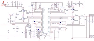
The project uses an LM5143 with 60V/20AH lithium battery input and 38V-53V/20A adjustable power supply output. The following is the design schematic diagram, please help to check it
Remove the low-side FET gate resistors - these are effectively never used (0Ω just compromised the layout and increases gate loop inductance).
Input ceramics should be 2.2uF/100V and placed close to the FETs (see EVM and app note SNVA803 for correct placement). One electrolytic for damping is set at 4x Cin (derated for voltage).
Tie mode directly to VDDA for 2-phase operation. 10k to GND is only used for lower Iq but compromises error amp performance.
No need for duplicate compensation components - 3 is sufficient on COMP1 (located close to the pin).
Same for RT and SS pins - one component on each pin. Multiple components will just degrade noise immunity on these high-impedance nodes.
Boot caps should be 100nF/25V or similar. 4.7uF is too high and stresses the boot diode at startup (not to mention it pulls down the VCC cap).
Boot diodes can be 75V/0.1A in SOD323 package or similar. Bigger than that will result in too much reverse leakage current at hot.
Not sure what these MOSFETs are, but 80V logic-level devices are recommended if Vin-max is 60V.