This thread has been locked.

If you have a related question, please click the "Ask a related question" button in the top right corner. The newly created question will be automatically linked to this question.

TPS55289: Copper Fill Under the Coil of TPS55289

Part Number: TPS55289

Hi everyone,

Recently I decided the use `TPS55289` for our LED driving application.

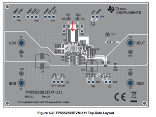
However, when I checked the layout recommendation of the IC and also evaluation board `TPS552892EVM-111` I realized that there are copper keep outs underneath of the switching coil.

After I done searching about the copper filling under the coil in switching regulators, most studies are showing that GND filling underneath of the coil is much better for EMC performance.

I have confusion after I checked the TI's recommendation in the attachment.

Could you please enlighten me?

  • Hi Alper,

    Thanks for reaching out and bringing this discussion.

    To give a conclusion, it is recommended to add the GND copper plane beneath the inductor for EMI consideration. And you can find more descriptions on the article below.

    https://www.ti.com/lit/eb/slyy208/slyy208.pdf

    About the EVM design, on the top layer, the cooper plane beneath the inductor was removed. But the GND plane is poured on the 2nd & 3rd & 4th layer for EMI consideration. We have not tried to compare the difference between GND copper plane beneath the inductor on top layer or not. But for molded inductors with terminations underneath the package, I think both are ok. From our experience before, many customers also cut off the copper plane beneath the inductor at the toper layer, and add GND copper planes on 2nd&3rd&4th layer.


    BRs,

    Bryce

  • Hi Bryce,

    Thanks for your detailed answer.

    I understand that there is no `must` situation here, we can either pour GND on the top layer or not, as long as we have inner GND layers, right?

    Thank you.

  • Hi Alper,

    Yes. From my understanding, inner complete GND layers are mostly recommended, and the GND copper plane beneath the inductor at top layer is not a must for shielded inductors.

    BRs,

    Bryce

  • Thx a lot Bryce!