This thread has been locked.

If you have a related question, please click the "Ask a related question" button in the top right corner. The newly created question will be automatically linked to this question.

TPSM5D1806: Help with very odd transient response...

Part Number: TPSM5D1806
Other Parts Discussed in Thread: TPS541620,

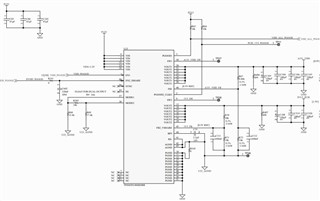
I am using the TPSM5D1806 in the following configuration:

VIN = 12V

VOUT1 = 0.9V (3A)

VOUT2 = 1.5V (2A)

1MHz switching frequency

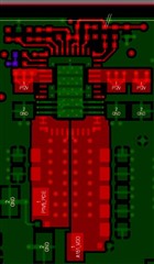
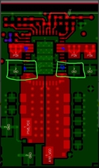
500uF output capacitance on 0.9V rail.

300uF output capacitance on 1.5V rail.

Both rails are stable during power up.

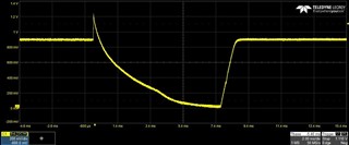
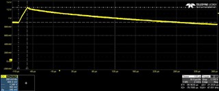
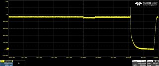
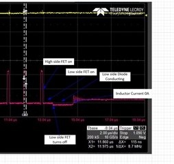
I am seeing the 0.9V rail spike (steady ramp from 0.9V toward 1.3V over 20ms) during current draw cycles (feeds the core voltage of a processor).

I monitor the SW1 pin and see pulses still going during this ramp (steadily decreasing in width).  The the regulator turns off then on.  My guess is the overvoltage on the output causes this.

What is going on here?????  If the current draw were to suddenly go from 6A to 0A then I would expect a short increase in output voltage due to loop response. However, I would expect it to respond quicker than 20mS.

I tried feedforward caps in parallel to the upper feedback resistor (47pF, 150pF, 470pF) and there is never a change to the output.

I tried running the supply at 500kHz switching rate, no real change to behavior.

I added another 600uF of ceramic capacitance to the output, no change.

Any help will be much appreciated.

-Kevin

  • Do you have a schematic, pcb layout and oscope waveforms?

    OV will cause the device to shut down for  > ~10ms before restarting. 

    Does the 1.5V have OV similar behavior?

    It is possible that there is a leakage path from 1.5V to 0.9V on the device being powered or on the board. 

  • David,

    Thanks for the quick response.

    Yes, it appears to be OV, yes it shuts off for 10ms then turns back on.

    Here is a screenshot from the scope:

    Close up:

    Pulses are measure on SW1 right up to the peak @1.2xV.

    1.5V is solid during this time.

    Here is a schematic:

    I can't conceive of a reason that would cause 1.5V to leak over into 0.9V only at certain times in the boot process?

    I have 3 other TPSM5D1806 devices on the card providing other voltages.  I only note an issue on this rail.

    In this screenshot from the scope you can see where the rail is being loaded briefly and doesnt appear to have an issue but then later the output spikes:

    Any insight would be most helpful...

    -Kevin

  • Here is a screenshot of parts placement in layout:

  • Note on schematic:  C111 and C112 are not populated

  • The placement on the input capacitors are good, but the GND pins, ground connections

    are not connected to the input capacitors like the vin pin connections (drawn green boxes).  

    The switching loop of the power stage will have more parasitic inductance versus a direct

    connection with a copper pour from the capacitor ground to the device ground on top layer. 

    Can the input voltage be measured at the blue dots during the OV event?   

    Also, during the OV event, can the TP27 SW1 be plotted with Vout.   

    Trigger on Vout with trigger at 1V, rising edge a normal or single trigger use a 2us/div. 

    I read the first message as 20milliseconds not 20microseconds, so I was thinking a leakage

    but in the microsecond range, I think the input supply maybe is affecting the control loop. 

    Has there been a A-B-A device swap experiment, to see if the issue follows the device or the board location. 

    If you have a device that is functioning as expected in a different location swap to this

    location and take the suspect device and place in another location. 

  • OK, there is a solid GND plane connecting everything on layer 2 but I see your point.

    Yes, I will measure 12V input at the blue dots during OV event.

    Yes, I can get a plot of TP27.  I tried to explain what I saw with this.  SW1 is still pulsing until the device turns off at the peak of the spike.  The pulses are getting thinner during this time but no skipping, etc...

    This is repeatable across multiple boards all with this same regulator showing the issue. It definitely appears to be specifically related to this rail of my design.

    Thoughts on running this at 1.5MHz?  Should I be looking at RS- or SS pins?

    Thanks,

    Kevin

  • For dual output configuration, the RS- and SS are not used.  

    With 1.5MHz switching frequency, Minimum controllable on time may cause the 0.9V rail to skip pulses.

    Also, check the AGND to PGND voltage. 

  • I will check that voltage (PGND to AGND) delta.

    I only ask to see if monitoring those pins would provide clues.

    OK, regarding 1.5MHz.

  • If I remember correctly, the SS and RS- pins mux'ed out of the circuit to use internal circuit or a node.     So I cant think of a way to use these pins. 

    FYI,  the TPS541620 is the converter used on TPSM5D1806.  

  • Here are some plots:

    1) SW1 and VOUT.  Switching stops after 20us when voltage gets to around 1.18V

    2) Zoom in on pulses. it doesn't look like the pulses are shrinking like I thought.  They stay around 115ns

    3) 12V (ac coupled) across the input cap during the 0.9V event

    4) VOUT2 (1.5V) during the 0.9V event.  AC and DC coupled.  Looks clean.

    I still owe you a pic of AGND to PGND but based on what I see on 1.5V I am not expecting a breakthrough there.

    Thanks,

    Kevin

  • If you look at the plot with 12V, the 12V starts to rise just as the rail starts the ramp from 0.9V to 1.118V. I assume from load current going lower.

    So, if rail is going from loaded to no load you might expect this peak.  A feedforward cap should have some impact here but I saw none in the three values I tried.

  • I think the rise in the input voltage at the 0.9V to 1.18V transient is from the device turning off

    from OVP and the device no longer pulling current from input and then input voltage rises. 

    The on time is 115ns in your measurement, I would expect the control loop to have on time to be ~75ns for 0.9V output. 

     With  1MHz switching frequency and 115ns on time, the control loop is trying to regulate to 1.38V,   Vout/Vin=ton*fsw.

    The zoomed in scope plot with vout and sw node shows the last pulse before OVP.   

    The high side fet is 115ns and then turns off and the low side fet turns on for a ~580ns and then LS fet turns off (OVP disables power stage).   

    Once the low side fet turns off, the low side diode conducts for ~1.2us since current is following to the load.   

    The inductor ramps down to 0A at that time the sw node rings.     

    If I assume the inductor ramps from a peak to 0A, during the last low side fet/diode conduction to the ring,

    using VL=L*dI/dt I estimate the inductor was greater than 5A.     So I do not think an unload transient is causing the OV.   

    The control loop for some reason has an incorrect on time.   

    On plots 3 and 4, the 0.9V (500mV/div) has a noticeable droop presumably from the output loading. 

    I would expect a smaller droop over the load and not visible with 500mV/div on a scope, but this change is visible.

    There are two control loops and I suspect the gnd could be the issue increasing noise in control loops.   


  • AGND and PGND showed no real perturbation during the 0.9V event.

    How can I pull this controller into webench and run simulation?

  • I am not sure why but the TPSM5D1806 is not enabled for the simulation in webench. 

    If you are interested in an EVM, I can send one. 

  • I will double-check webench available resources. Do you have recommendations to improve our control loop?

  • Another piece of information is that this design seems to work as the same circuit and layout for other voltages in other locations of the board but for some reason this specific rail has issues. Lastly, the one main difference for this rail is that it is the lowest voltage compared to the others.

  • I have the EVM.

    The pulses measure 103ns when output voltage is at 0.9V.

    The pulses grow to 121ns before OV shutoff.

    The feedback node shadows the output voltage.  i.e. pulse width is growing as the feedback voltage is rising? Feedback pin is going higher than 0.5V during the ramp from 0.9 to 1.18V as the pulses are getting longer...

    How is it getting into this mode?

  • I tested my evm with 0.8v, 0.9V and 1V with 12V input and 1MHz and did not have this issue up to full load.   

    I will test tomorrow beyond 6A and see if there is any strange behavior when entering current limit.  

    Also, has a known good device from another location on board been placed in the 0.9V position

    and the problem 0.9V device been placed in the other location to check if the issue follows the specific device. 

    Usually the lower rail voltages have the higher currents, what are you expecting for the peak current for 0.9V.  

  • Expecting less than 4A.  I would not be surprised if for short timeframes it was higher.

    This part is used in three other locations to create the following:

    1.8V @ 1-2A & 1.1V @ 3-4A (parallel out)

    1.35V @ 3-6A (combined out)

    1.2V @ 1-2A & 0.9V @ 2-3A (parallel out, we have not seen an issue with this 0.9V rail but have not been able to exercise it fully due to the issue with the other 0.9V powering the processor core preventing full functionality)

    The same rail on multiple assemblies is showing the same behavior.  I don't think this is one bad egg out of the bunch.  Maybe something really obscure with the layout of this particular rail but nothing sticks out to me when I review it.

    What would cause the controller to go open loop like this and lose control of the 0.5V control point it is trying to maintain?

  • I reviewed the incident with my supervisor and he is perplexed as well.    We came up with additional questions to clarify our assumptions.     

    What are the specs for the 150uF electrolytic and has any testing occurred without it. 

    To increase the loop bandwidth, reducing the output capacitance can increase the response time.   Cout has be increased  and tested, has any testing occurred by reducing cout. 

    When there is unexplainable behavior, the PCB layout and noise sources are suspects.

    Can a scope plot of the FB1 pin to AGND pin without bandwidth limit, dc coupled be captured. 

    As well as, AGND pin to PGND pin without  BW limit 

    and FB1 to PGND.     

    The grounds of the input capacitor near PGND pin 10 and PGND pin 29.

    Where does the R67 high side feedback resistor connect to the output capacitor: closer to IC or the load. 

    Also, if you have a TPSM5D1806EVM  link can you test the 0.9V schematic on the evm.   

    If you do not have, I can send you a board. 

  • Yes, I tried removing the 150uF electrolytic and no change.  I tried this before adding more bulk for the same reason you noted above.

    Other than removing the 150uF electrolytic (which had no effect), no other caps were removed.

    R67 connects closer to the IC.

    I can get the scope plots you are asking about.

    I am not sure I can replicate the load with the EVM.  Are you asking to tie the EVM output into the CCA?

  • I am not suggesting at this moment to tie into the system, but only to validate the schematics bill of materials and the problem device on the evm.

    The schematic is not much different than other BOMs I have tested and you already remove/added cout as an experiment, so I expect no surprises. 

    Ideally, if the problem device is installed on the evm with the current schematic.     

    There are probably many events going on the system board that the evm will not have: ground plane currents, noise etc. 

    If adding the evm to system is possible, the output current could be measured with a current probe and the

    device could be isolated from noise, etc from the system board, it may be worthwhile experiment 

  • If any additional information is needed, please post or click resolved 

  • We are still reviewing the issue.  No resolution at this time.  I am investigating wiring in the EVM output into the CCA.

    Here is a plot of FB1 (blue, AC Coupled) and VOUT (magenta).  I did limit bandwidth on the scope but I can take another capture, based on what I see here though I can't see how that would uncover anything. 

  • The FB and VOUT waveforms definitely show the cause of the OVP, but the root cause of the OVP is elusive to me. 

    The ramp and clock determine the turn on and termination of the pulse width and noise can have an effect on the

    switching but I have not seen such a response on this device.   The evm experiment may be the easiest way to troubleshooting the issue.