This thread has been locked.

If you have a related question, please click the "Ask a related question" button in the top right corner. The newly created question will be automatically linked to this question.

UCC21755-Q1: I am having issue with my gate drive output

Part Number: UCC21755-Q1

Hello

Please, I am having an issue with my gate drive output where one signal looks higher than the other.

Here is the trace:

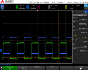
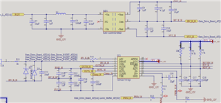
The green is high-side gate drive with +10/-10V.

Blue is low-side gate drive with +20/-5V.

My problem here is that the green gate drive has a very low Vgs. I would like to know why I am seeing this and what the cause of it is.

I was expecting the same voltage as the blue trace. I have measured the power supply for VDD and VEE. The VDD is showing me +19.4V and VEE -6.51V (green trace), and the blue VDD is +20.5V and -5.1V.

I need some help here, please.

I am using a differential probe with x10 on my measurement.

Regards,

Ikenna.

  • Hi IKenna,

    Thanks for your interest with UCC21755 device,

    Is it possible to capture both VDD and OUT in a single plot for both high side and low side? Also where is the OUT measured close to device or close to the GATE? What is the gate resistance used in your system?

    Thanks

    Sasi

  • Hello Sasikala,

    I measured the VDD with respect to the common pin, and I measured +20/-5 on the blue trace, which is the low side (LS), and +19.8/-6.51 on the high side (HS), which is the green trace.

    The gate resistor I use is 1 ohm because the MOSFET has an interresistor of 2.4 ohm. How do I know if my gate driver is damaged? What is pulling the green trace to +10/-10V?

    All your gate drives failed so much, and when I measure, the temperature is just below 70 degrees. I have a clean signal into the input of each gate drive (HS and LS).

    The HS is where the problem is right now.

    Regards,

    Ikenna.

  • Hi Ikenna,

    Its had to explain, unless you share the schematics and the actual captured waveforms.

    In the attached image, what is the HS (green waveforms) voltage/div -> it says 1V/div, it doesnt represent +/- 10V .Can you explain why?

    Can you please share VDD and OUT (high side) measurement in a plot? Hope you are using differential probe as Highside ground (COM) is not "earth ground"

    Have you got the system working before or you are trying to bring up for the first time.

    Thanks

    Sasi

  • Hello Sasikala,

    I use an X10 differential probe, and the voltage/div is 1V. If you multiply it by 10x1, it'll give you 10V. I am measuring VDD with respect to the common pin in the isolated power supply.

    I am trying to bring it up. What can cause a gate drive failure?

    Regards,

    Ikenna.

  • Hello Sasikala,

    I just measure the green trace. When I am not switching the gate drive, it stays at +20/-5, and as soon as I switch, it drops to +10/-10. That is for the green trace.

    That the schematic.

    Regards,

    Ikenna.

  • Is there anything that can be pulling it from +20/-5V to +10/-10V.

    Regards,

  • Hi Ikenna,

    No the output should be either VDD or VEE, not +/-10V. 

    That's why it will be helpful to capture the VDD during the switching along with OUTH - also please confirm if you are using differential probe to measure high side gate output.

    Thanks

    Sasi

  • Hello Sasi,

    Yes, I am using a differential probe to measure the OUTH. I am trying not to use a passive probe or short anything. I will capture the result you asked for and share it with you.

    Regards,

    Ikenna.

  • Hello Sasi,

    The OUTH is going now to +20/-5V. This was after I took off Rg_ON and measured directly from the output. I would like to know why when it is connected to the MOSFET through Rg, it goes to +10/-10V, and when I remove Rg, it goes straight to +20/-5V.

    Do you know what it means to pull it to +10/-10V?

    Regards,

    Ikenna.

  • Between gate and driver output, there is only gate resistor right??- So it shouldn't vary from +20/-5 to +/-10V, It also doesn't seem like shifted as, net 25V becomes net 20V - which is unexplainable.

    Can you please measure each node away from gate driver output pin, to understand where it is changed?

    Thanks

    Sasi

  • I want to test the output without the MOSFET because I do not want to damage it. I would prefer testing it in a separate way. Is there anyway I can test my gate drive without the MOSFET? If that would make me see the same issues.

  • Sure you can disconnect the mosfet and plan a capacitor as load for the gate driver - capacitor value can match the mosfet's input capacitance.  However based on your prior testing - without gate resistor connected, you could measure the gate voltage reflecting appropriate value. So I believe that some components on the Gate is causing this behavior. As you have not shared the entire circuitry, I couldn't comment about it. If possible please share schematic section of OUTH, OUTL to the mosfet, to double check for anything obvious.

    one more thing you could check- how is the CLMPI pin connected to Gate- I believe directly to the gate without any component in between - is it right?

    Thanks

    Sasi

  • Hello Sasi,

    I am happy to share the full schematic with you, but because of confidentiality, I won't be able to do it here. If we can get a private chat, I can send the full schematic to you. I know I have had a private chat with your colleague and will share my schematic with them.

    Regards,

    Ikenna.

  • Hi Ikenna,

    I have emailed you from my company email id, you can share the schematics there. 

    I will close this email thread.

    Thanks

    Sasi