This thread has been locked.

If you have a related question, please click the "Ask a related question" button in the top right corner. The newly created question will be automatically linked to this question.

TPS6521905: TPS6521901 - AM6442BSEFHAALV

Part Number: TPS6521905
Other Parts Discussed in Thread: TPS22965

Hi Team , 

We are using PMIC TPS6521901  for powering  AM6442BSEFHAALV   .   We are in the board bring up stage but struck with the PMIC powering up . We are using 5V input and the enable pin is tied to 5V.   but PMIC is not responding . TPS6521901_pmic_Arm64x.pdf

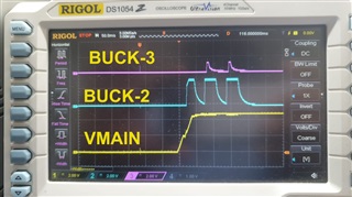
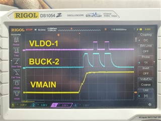
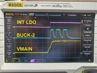
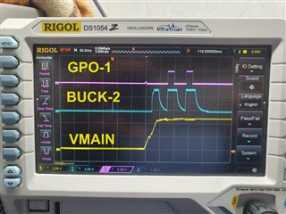
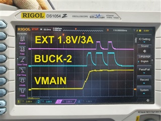
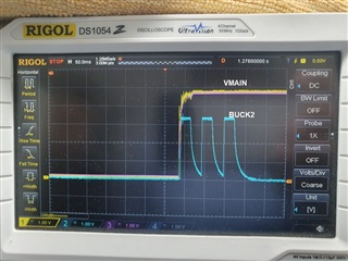
Please see the attached schematics used .     
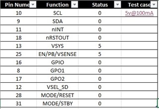
. We tried to isolate the output rails by disconnecting the zero ohms in the o/p rails 

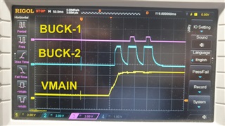
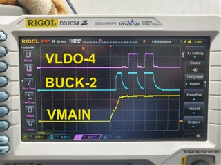
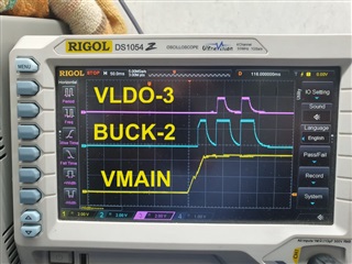
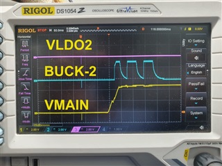
The voltages measured at each control pin is also listed . Kindly go through the schematics and share some lights . 

What shall be the minimum current  from the input supply   to start functioning the device ?  The input current is measured as 4 mA   only now .    

The source current is limited to 500mA   for the test purpose (no load is connected) 

  • Hi,

    Thanks for reaching out. Please find the feedback below and let us know if you have any questions. 

    • The DNI resistor connected to the output of the VLDO1 must be placed after the output capacitor. VLDO1 is part of the PMIC power-up sequence and requires the 2.2uF output cap to be present. 

    • What are you supplying with "VCC_3V3_SYS" and what is the total current needed? why there is a separate discrete Buck suppling 3.3V to the same net?

    • What is TPS22965_EN connected to?

    • The PMIC GPO2 is disabled by default on the TPS6521901 NVM. This means the device will have this pin internally pulled down. It can only be released by sending an I2C command after the PMIC finishes the power-up sequence.

    • Where is the external pull-up resistor for GPO1 (EXT_PWR_EN)?

    Thanks,

    Brenda

  • hi Brenda , 

    Thanks for the response . 

    • We have tried the VLDO1 capacitor placing befor the DNI resistor , still PMIC is NOT responding 
    • "VCC_3V3_SYS"   need tp source around 1 A  and that is why external Buck is used . We were planning to isolate the PMIC LDO out put with the DNI resistor . 
    • TPS22965_EN   is pulled up to external 5 V (VMAIN)   and we could measure 5V  at the PMIC pin
    • The PMIC GPO2   is not using and Pulled up to VMAIN (5V)  now 
    • GPO1 (EXT_PWR_EN)  is not connected to pull up resistor now 

    VMain  5V   current is limited to 100mA   for the test purpose (no load is connected)   . What shall be the minimum current  from the input supply ?

    Few additional observations 

    While measuring resistance with GND  we found following rails have low resistance , we would like to know if this characteristic is ok or for the processor (AM6442BSEFHAALV)?

    VDD_CORE --- 20R

    VCC_3V3_SYS --- 78R
    VLDO2 --- VDDR_CORE --- ~190R

  • Hi,

    Thanks for sharing the information! Here are my next questions:

    • How was the VLDO1 capacitor placed before the DNI resistor? Did you update the schematic/layout and built a new prototype board?

    • What are you supplying with "VCC_3V3_SYS"? What's the difference between the external 3.3V Buck and the PMIC Buck2?

    • If you are measuring 5V on TPS22965_EN (GPO2), then the PMIC is not working and might be even damaged because GPO2 is disabled by default on the TPS6521901 NVM. This pin can only be enabled/released by I2C.

    • If you don't have a pull-up resistor on GPO1 (EXT_PWR_EN), then the 1.8V IO (VCC1V8) wont meet the sequence requirements of the processor. 

    • Could you provide a power-up scope capture of the signals listed  below? Please use a time scale of 4ms or close.
      • VMAIN (PMIC VSYS)
      • SoC_DVDD3V3 (PMIC Buck2)
      • VLDO1 output
      • VDD_DDR4 (PMIC Buck3)

    Thanks,

    Brenda

  • Hi Brenda,

    • Two approach we made here with the board 1. soldered the DNI resistor so that the capacitor is now connected . We removed R873 to isolate the discrete  buck U17.  2)  soldered a 2.2uF near the PMIC pin on DNI resistor pad and GND with a extra short wire   , Both case did not worked 
    • PMIC buck2  is used to power SOC and LDOs  of PMIC only . External 3.3V buck is used to power some peripherals like Jtag ,Ethernet, one external card etc 
    • TPS22965_EN (GPO2)   is pulled up to Vmain , it is reading Zero ( sorry for the mistake ) . This pin is not using to control any devices.
    • We shall be soldering  one pull up resistor in GPO1 (EXT_PWR_EN)  and update the result . 
    • Kindly share your views on input current and the lower resistance observed on power rails .  Is it safe to increase the input 5V current to 2~3A range ?


  • Hi,

    I would recommend verifying the 3.3V signal split (between PMIC Buck2 vs external discrete) with the processor team. All signals (attached devices) connected to these IO domains must be powered from the same power source that is being used to power the respective processor Dual-voltage IO domains (VDDSHVx supply rail). A valid supply voltage for the VDDSHVx supplies must be present before any input is applied to the associated peripherals or IOs. This affects the sequence of the rails supplying 3.3V. 

    The input current requirements are specific for each application based on the expected total current on each rail including PMIC, processor and peripherals. To get an estimate of the required input current for the PMIC, I recommend using the PMIC efficiency and thermal estimator at the following link: https://www.ti.com/tool/download/SLVRBL7

    Thanks,

    Brenda

  • VDD1P8 should have 1.8V after the pre-regulator is connected to the VSYS pin (even if the PMIC enable pin is low). It would be very helpful is you could provide the power-up capture we had requested on a previous message. The scope captures in your message do not show the power-up and we need to see the ramp of the 5V supply. Could you capture the 4 signals below (or at least the first three) with a small time scale (~4ms)? We need all signals in the same scope capture. 

    • VMAIN (PMIC VSYS)
    • SoC_DVDD3V3 (PMIC Buck2)
    • VLDO1 output
    • VDD_DDR4 (PMIC Buck3)

    Please also increase the current compliance of the 5V supply.

    Thanks,

    Brenda

  • Thank you Brenda . We shall get the required data soon

  • awesome. In the meantime, we are changing the state of this E2E to "waiting for customer". 

    Thanks,

    Brenda

  • Hi Brenda 

    Please see the below wave forms . All captured in 50ms time. VLDO2  is powered by external 1V8  , which is enabled by GPIO1  


  • Thanks for sharing the scope captures. Here is the feedback:

    • The ramp of the "VMAIN" supply is very slow and doesn't meet the required voltage level when Buck2 is turned ON. For example, Buck2 is configured to output 3.3V and the PMIC data sheet specifies a voltage headroom of approximately 400mV to 700mV. That means the voltage on VMAIN must be at least 3.7V-4V at the time Buck2 is turned ON.

    • The output voltage on VLDO1 doesn't match the expected value. If the VSEL_SD pin is connected to a pull-up resistor, then VLDO1 is expected to output 3.3V. 

    • It seems like on the second power-up attempt, all PMIC rails except LDO2 are able to ramp. Could you take a scope capture including the LDO2 input and output (PVIN_LDO2 and VLDO2)?  

    Thanks,

    Brenda

  • Hi Brenda , 

    Thanks for the comments

    • LDO2  is powered by external 1V8  . This regulator is enabled by GPIO1.. Below is the wave form of 1v8.   currently .LDO2  is not giving any output
    • VMAIN ramp up issue we are studying and update you .
    • VLDO1 issue is because , the pull up is powered from VCC_3v3_SYS  , which is now OFF   and the VSEL_SD pin  measures 0V now.


  • Hi Brenda,

    here is the update

    1. Regarding the VMain ramp up issues , we rectified the slowness still BUCK2 and other rails performance remained the same.

    2. Since the PMIC is trying to turn ON  3 times and shuts down - the reason would be any of the non maskable faults ? Are you suspecting over current  can be the reason ? Your suggestion on testing these cases would be very helpful . We are now isolating all the rails from the load and testing it.

  • I would recommend testing the power-up sequence with all the output rails disconnected from the load. 

    Did you increase the current capability of the input supply based on your power analysis at the system level and the expected maximum current consumption?

    Thanks,

    Brenda

  • Hi Brenda , 

    I would like to update the followings and get your thoughts . We have 2 boards under test

    After implementing the GPO1 pull up and correcting the external 1V8 buck output ( supply for LDO2)  , PMIC started working . 

    Unfortunately in one board  while loading "VCC_3V3_SYS"  , (generated by an external Buck U17 ) is showing very low impedance and draws high current (we are suspecting short with some ICs) . This collapsed the whole system . This rail do not have any direct connection with PMIC  . This supply is used for EMMC , JTAG , and some buffers etc. After this rail loaded , PMIC started to misbehave , Not getting any outputs . It tries to turn on BUCK2 3 times and goes OFF. We isolated the "VCC_3V3_SYS external buck from the system , still PMIC  is not responding .  Please see the below waveform . No there rails are trying to turn ON . Internal LDO (pin14 ) is working . 

  • Hi,

    We need to understand how the 3.3V load is distributed between the PMIC Buck2 and the external discrete and get the full schematic reviewed by the Sitara processor team to make sure your application meets the MPU requirement listed below.

    "All signals (attached devices) connected to these IO domains must be powered from the same power source that is being used to power the respective processor Dual-voltage IO domains (VDDSHVx supply rail). A valid supply voltage for the VDDSHVx supplies must be present before any input is applied to the associated peripherals or IOs."

    How may failing and passing boars do you have? Are they all identical? Did you implement the fixes (like GPO1 pull-up, external 1.8V, etc) in all of them? 

    Thanks,

    Brenda

  • Hi Brenda, 

    I would like to update the issue is resolved . Performed the  GPIO pull up fix and fixing some  assembly issues resolved the problem

  • awesome! Thank You for letting us know the issue was resolved. We will close this E2E for now but feel free to submit a new one if additional support is needed. 

    Thanks,

    Brenda