This thread has been locked.

If you have a related question, please click the "Ask a related question" button in the top right corner. The newly created question will be automatically linked to this question.

TPS650864: Efficiency and thermal calculator

Part Number: TPS650864
Other Parts Discussed in Thread: CSD87381P, TPS650861

Hi

We are designing our Video Processing board using Xilinx Ultrascale FPGA XCZU3CG-L1SFVC784I.We are designing for low power.

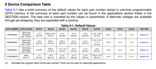
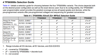
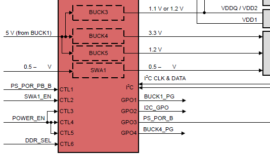
We are planning to use TPS6508641 to power this.

  • We want to do thermal analysis to check if junction temperature is within limit. Please let me know if there is any calculator for this.
  • Any heat sink would be required?
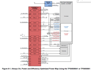
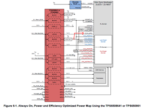
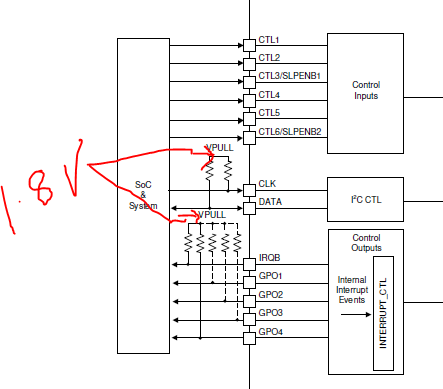
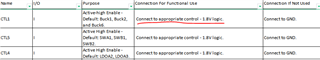
  • There is no 3.3V from PMIC connected to the FPGA in the implementation in doc SCEA113, sec 6.1. How to interface FPGA with peripherals which are operating at 3.3V?
  • Hi Prema,

    • For thermals, all we have is a Flotherm model on the main product page. We don't have a thermal calculator: https://www.ti.com/lit/zip/swcm008
       
    • You don't need a heat sink for this PMIC, just make sure the PGND pad is fully connected to the PCB and provide multiple vias to the pad.
       
    • I'm not sure what's required for FPGA to peripheral connections. The reference design above is used to supply power from the PMIC to each device but interconnecting the FPGA and peripherals is outside the PMIC domain.

    Regards,

    James

  • Hi

    Thanks for your response. We want to compute the total power consumption for our design and hence looking for a calculator.

    • Please share with us reference design for PMIC TPS6508641 powering Xilinx Zynq UltraScale+ FPGA.
    • Also please let us know the difference between TPS6508641 and TPS6508640. Which would be suitable for powering XCZU3CG-L1SFVC784I?
    • For buck1,2,6 is CSD87381P required? what is the output current of buck 1/2/6? We want to know so that we can decide if this current booster is required or not.
  • Hi Perma,

    • I believe the reference design you are looking for is TIDA-01393
       
    • The main differences for the TPS650864x PMIC versions are listed in the datasheet Table 5-1

       
    • The application note Using TPS65086x PMIC to Power Xilinx Zynq UltraScale+ MPSoCs has a table for selecting the PMIC version you want to use:

       
    • CSD87381P is the recommended external FET selection but you can use any of the options in the datasheet section shown below depending on your current requirements. The output current depends on your FET selection since the FETs are external for BUCK1, 2 and 6.

    Regards,

    James

  • Hi James,

    In the below implementation, VCCO_HPIO and VCCO_PSIO are connected as dotted lines. Is it because they can be changed?

     I'm asking this because VCCO_HPIO is at 1.2V and we require 1.8V. Can we connect o/p of buck 6 to it to operate at 1.8V?

    Please let us know.

  • Hi perma,

    The dotted lines indicate optional connections. You can connect the 1.8V to this line from BUCK6 as long as you have enough current budget from BUCK6 for this input and the power up timing recommendations of the Xilinx are still being followed.

    Regards,

    James

  • Thanks James,

    What is the power sequence for LDOA2 and Buck 6 in the PMIC? do they come up simultaneously ? Please let me know. 

  • Hi perma,

    Please see the datasheet Figure 8-11 for power sequencing on the TPS6508641. LDOA2 is tied to BUCK6 power good so LDOA2 will not ramp up until BUCK6 ramps to the target voltage successfully.

    Please note that currently, LDOA1 should come up AFTER BUCK4 as it is tied to the BUCK4 power good signal. We are working on updating this part of the sequence.

    The TPS650861 is user programmable so the power sequence can be adjusted as necessary.

    Regards,

    James

  • Thanks James

    One another query. Our input voltage is 2.5V to 17V. The PMIC Vin min is 5.6V. Hence we are looking for a suitable buck boost to provide this min vin voltage to PMIC. Please suggest some suitable parts.  current rating 2-3A.

  • Hi perma,

    I would recommend taking a look at the buck-boost categories here: https://www.ti.com/power-management/buckboost-sepic.html

    There are some mid and wide VIN options that may be of interest. After checking each section, it look like only the wide VIN options would cover the range from 2.5V to 17V but some of these are automotive grade parts which may increase the cost and it doesn't look like the max current output would meet your needs.

    I'm not as well versed in the discrete buck-boost catalog so I recommend creating a separate E2E post to get a discrete BUCK-BOOST recommendation from someone who works closer to these devices.

    Regards,

    James

  • Thanks James

    We are doing power calculations and we require efficiency for the various bucks. However, we are not finding this detail in datasheet.

  • Hi perma,

    You can use the below figures from the datasheet to estimate efficiency for all the BUCKs. Use the BUCK1 efficiency to estimate for BUCK2 and BUCK6. Use the BUCK3 efficiency to estimate for BUCK4 and BUCK5:

    BUCKs 1, 2 and 6 have matching architecture and BUCKs 3, 4 and 5 are the same so efficiency differences should be minimal at the same operating points for both groups.

    Regards,

    James

  • HI James

    Thanks 

    We are computing the power dissipation for the PMIC and found it to be high around 2Watts. 

    Following are the currents for the various regulators. Please let us know what would be the power consumed by PMIC.

  • Hi perma,

    Let me take a look and I'll get back to you early next week. I have some urgent lab testing today.

    Regards,

    James

  • Hi James

    Any update on our query?

  • Hi perma,

    If the power dissipation seems high, I would double check the calculations using the equations from the below resources:

    https://www.ti.com/lit/pdf/slva390 - Includes power dissipation formulas for bucks

    E2E Thread - Includes information about LDO power dissipation

    Regards,

    James

  • Hi James

    I'm unable to access the e2 link for LDO power.

    Another query is : We need to supply 1.8V for peripherals at 0.46A. The SWA1 has a current rating of 300mA only. 

    Please let us know which buck/ldo we can use for 1.8V for peripherals. 

  • Hi perma,

    The E2E thread just mentions that LDO power is calculated using P = (Vin - Vout)×Iout.

    The first page of the datasheet shows the current and voltage capabilities of each output.

    Regards,

    James

  • Hi James

    Can SWB1_2 of TPS6508641 be used for connecting 1.8V to peripherals? Is the power sequence of this similar to SWA1? 

    The current output of SWA1 is not sufficient and hence we want to use SWB1_2 in addition to  SWA1. 

  • Hi perma,

    SWB1_B2 can provide a combined total of 800mA current which would be more than enough to meet your 0.46A requirement.

    SWB1_B2 powers up from CTL5 and requires BUCK4 Power Good before it will be enabled. This is different from SWA1 which only depends on CTL2

    Regards,

    James

  • Thanks James. So we can use SWB1_B2 to power peripherals working at 1.8V. Is that rite?

    I understand the sequence of SWB1_2 is after BUCK4.I would like to know, 

    What is the sequence of SWA1? It is based on which power good signal? 

  • Hi prema,

    SWA1 is not based on a PGOOD signal, it only requires CTL2 to be high.

    Yes SWB1_B2 can power your peripherals at 1.8V.

    Regards,

    James

  • Thanks James.

    • Can we connect 1.8 V (from BUCK6) to the input of SWB1_2?
    • What is the Vgs driven to CSD87381P from the PMIC internal buck? We need this to compute power dissipation of CSD87381P. 

    Please let us know

  • Hi Prema,

    Due to the holiday in the US, many of the device experts are currently out of the office. When they return they will look into this and provide a response. Please expect some delay accordingly.

    Thanks,
    Field

  • Hi prema,

    • You can connect BUCK6 to the input of SWB1_B2 as long as SWB1_B2 is enabled after BUCK6 is ramped up. If SWB1_B2 tries to ramp up before the input voltage is available, you will get a power fault and the PMIC will reset.
       
    • Gate driver for the FETs use the 5V input to the DRV5Vx pins of the PMIC so Vgs should be essencially 5V. The bootstrap circuit uses an active internal diode so the voltage drop from the 5V input is very small (likely 70mV or less when charging the bootstrap capacitor).

    Regards,

    James

  • Hi prema,

    I made some edits to my response above after looking into the device a bit more and accounting for the active diode on the bootstrap circuitry.

    Regards,

    James

  • Thanks James. 

    I understand that SWB1_2 uses Buck4 PG as enable and to use buck6 as input voltage, the SWB1_2 should not be enabled(buck4 PG) before input voltage(buck6 vout) is available. So the below configuration to connect 1.8V to peripherals would work depending on the sequence between buck 4 and buck6. Can you please let us know what is the powerup sequence between these buck4 and buck6? Is there a chance buck4PG would be present before buck6 is available in TPS6508641 ?

  • Hi prema,

    BUCK4 depends on LDOA2 PG and LDOA2 depends on BUCK6 PG. Therefore, BUCK4 should never enable before BUCK6 is ready.

    Regards,

    James

  • Hi James

    Thanks, now I'm sure that I can connect 1.8V from SWB1_2 to Peripherals using Buck6 as input.

    I have a couple of more queries,

    • 0.85V from CSD87381 can be connected directly to pins VCCINT_IO, VCCBRAM, VCC_PSINTLP, VCC_PSINTFP ? Similarly other outputs from PMIC(except those marked with filters), can it be directly connected to the respective pins as shown in Figure 6-1 of doc scea113? Or is there any other component like load switches in between ?
    • please let us know the beads to be used in the filters recommended for VCCADC,VCC_PSADC,VCC_PSINTFP_DDR pins of the zync ultrascale.

    Please share, if there is any reference schematics with PMIC TPS6508641 interfaced to Zync ultrascale+ 

  • Hi prema,

    • The outputs can be connected directly as shown in Figure 6-1 without any additional devices in between. All you need are the passive components (output inductor and output capacitors) for each regulator.
       
    • We don't have a specific recommendation for the filters or beads you should use. We advise using a low pass filter for those pins but the decision of what filtering method and values to use is left to the board designer. This filter choice will depend on what frequencies are the most problematic on your board design.

    Regards,

    James

  • Thanks James

    I want to know

    • if the I2C and GPO signals can be pulled up to 1.8V, as all the FPGA banks are operating at 1.8V and these signals would be connected to FPGA.(below image)
    • Is it possible for any PS FPGA bank to be powered with 3.3V from buck4 of PMIC? We have very few signals from peripherals at 3.3V and want to know if these can be directly connected to FPGA PS GPIO instead of using a level shifter.

  • Hi prema,

    • The GPO and I2C pins can be pulled up to 1.8V. Depending on the 1.8V source timing you may need to wait for the 1.8V rail to ramp up before the pull-up can be applied to the I2C and GPO pins. Keep this in mind if you see any timing issues with the GPOs or if there's I2C communication you need soon after system power up.
       
    • I'm not exactly sure what you mean here. If this is a question about the processor capability you may need to ask on the processor support side of things. BUCK4 should be available for whatever usage you see fit as long as you're not exceeding the current capability of the BUCK4 output.

    Regards,

    James

  • Hi James

    Please let us know,

    • if we can give pullups for GPO output pins to 1.8V which is output of Buck6 instead of LDO3P3, as all FPGA banks are operating at 1.8V.
    • What is this signal I2C_GPO ?
    • DDR_SEL should be pulled low or high to operate at 1.1V for lpddr4?
    • We are using LDO3P3 to pull up the input CTL signals(PS_POR_PB_B,SWA1_EN,POWER_EN,DDR_SEL).Please let us know if this is fine.
  • Hi Prema,

    James is out of office today but he will be able to look into your questions when he returns on Wednesday 6/12.

    Best regards,

    Matt

  • Hi prema,

    • 1.8V can be used for the GPO pull-up source
    • GPO2 can only be enabled through an I2C command on the TPS6508641. This is why the GPO2 output is labeled as I2C_GPO
    • 3.3V is also fine for all CTLx inputs

    Regards,

    James

  • Hi James

    • We are following Implementation as per fig 6.1. Here DDR_SEL is mapped to CTL6. We want to know how to set Buck 3 o/p to 1.1V ,as it has the option for 1.1V or 1.2V.I had an understanding that DDR_SEL pin is for selecting this voltage level for buck3. Please let us know.

    • Another query is whether we can use Buck 6 output to power 1.8V to peripherals in addition to FPGA, instead of using SWB1_2. 
  • Hi prema,

    Sorry, you are correct above. CTL6 is DDR_SEL which is the SLP voltage control pin for BUCK3. BUCK3 will be 1.1V when CTL6 is pulled high. When CTL6 is pulled low, BUCK3 voltage becomes 1.2V. I may have been looking at a different IC version earlier.

    BUCK6 should have more current capability than SWB1_2 so I don't see an issue with using BUCK6 for 1.8V peripherals. BUCK6 power up sooner than SWB1_2 in the power sequence so as long as this is acceptable in your system you can switch to BUCK6 for your 1.8V source.

    Regards,

    James

  • Hi James

    Please let us know regarding the following

    • Is VPS_MGTRAVCC 0.9V? Because datasheet of FPGA recommends 0.875V max.
    • In PMIC checklist document we are seeing CTL to be connected to 1.8V logic. However we are using pullups to 3.3V similar to eval board design. please let us know regarding why its mentioned as 1.8V in checklist.
  • Hi prema,

    Regards,

    James

  • Hi James,

    Thanks for sharing the link.

    In that link we noticed that Buck 6 is not recommended for powering VCCO_HPIO. 

    Is this of any serious concern? please let us know as we received feedback from you previously that we can connect buck6.

  • Hi prema,

    BUCK6 power up sooner than SWB1_2 in the power sequence so as long as this is acceptable in your system you can switch to BUCK6 for your 1.8V source.

    The main concern with BUCK6 is the timing. BUCK6 powers up before SWB1_2 so if this violates the timing spec of your processor I would just make sure that the processor can handle the change. The BUCK6 itself can support the power rails needs but the processor may see increased power up current or other change in power consumption depending on the power up timing.

    Our recommendation is to follow the power timing first so it's up to you if you want to use BUCK6 for VCCO_HPIO or not.

    Regards,

    James

  • Hi James

    What should be the best value for Vin to PMIC and external mosfet(CSD87381P) for better efficiency and w.r.t thermal dissipation.

    The reference design is based on 12V Vin. and as per PMIC datasheet Vin min required is 5.6V.

    I want to know if 6V Vin is better or 12V Vin? or any other voltage is better pls specify.

  • Hi prema,

    Lowering the VIN voltage will improve the efficiency for the BUCKs in general. For the BUCK converters you may see less efficiency at higher load currents but for BUCK1, 2, and 6 lower VIN should give better efficiency across a wide range of load currents (See the difference between Figure 7-4 and Figure 9-8 in the datasheet). 6V should improve efficiency for the same VOUT, IOUT, and inductor value.

    Power loss is a bit more difficult to determine as there are a large number of factors at play in a synchronous buck (See An Accurate Approach for Calculating the Efficiency of a Synchronous Buck Converter Using the MOSFET Plateau Voltage)

    Lowering the input voltage reduces the power loss in a number of metrics but also leads to an increased duty cycle. The increased duty cycle can raise your power consumption in certain metrics. Usually, lowering VIN results in a net reduction in power consumption and, in general, the trend seen in electronics is to reduce the required input voltages for a given system.

    Regards,

    James

  • Thanks James

    We will go with 6V input to PMIC. We are giving the same Vin of 6V to the external mosfets also?

    Is 6V input to the external mosfet CSD87381P fine

    Regards

    Prema

  • Hi Prema,

    James is out of office until Monday 7/8. He will be able to answer you question when he returns.

    Best regards,

    Matt

  • Hi prema,

    Yes, 6V should be fine for the FET inputs.

    Regards,

    James