This thread has been locked.

If you have a related question, please click the "Ask a related question" button in the top right corner. The newly created question will be automatically linked to this question.

TPS563249: Regarding abnormal operation of TPS563249DDCR

Part Number: TPS563249

When we checked the power waveform of the circuit using TPS563249DDCR, we found the following two abnormal operations. Please tell me the causes and countermeasures for each.

circuit diagram

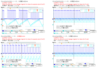
①L1 direction = positive direction There is abnormal operation (intermittent oscillation).

②L1 direction = opposite direction Although it is continuously oscillating, the output voltage (setting = 5V) has become approximately 5.1V.

  • Hi smash,

    The inductor direction affects your stability, so it maybe SW noise disturbs the FB pin. You can upload your layout here for us to analyze. But a 22uH is not suitable here, we recommend 1-3.3uH here and the rated current of your inductor is 2A, so don't test above this. 

    You can also try to add a 10-47pF on C6 to see if any improvement.

    Thanks.

    Regards,

    Shipeng

  • Dear Shipeng Cheng, Thank you for your reply.

    In order to reduce the output voltage ripple, the inductance was increased.

    I understand that an inductance of 22uH is not suitable, but could you please tell me specifically what kind of abnormal phenomenon you are concerned about?

    I will also send you the layout, so please check it.

    TPS563249 circuit layout.pdfthank you.

  • Hi smash,

    What is your goal of ripple? You can see in the datasheet our ripple is only 10mV using a 1.5uH inductor.

    The loop compensation is fixed and integrated inside our device. It cannot be suitable for all condition so the external components should be within a range.

    I review your layout and find some problems: 1. SW node is long and thin, which can cause much noise around the device. 2. the FB node wire is long, which will sense more noise. 

    You can first try to change the inductor. Thanks.

    Best Regards,

    Shipeng

  • Dear Shipen Cheng, Thank you for your reply.

    Transmit the data by changing the inductance.

    Simply changing the inductance to 3.3uH did not resolve the abnormal operation (intermittent oscillation).

    The continuous oscillation phenomenon was also observed at 22uH when the direction of L1 was reversed.

    At this time, the output voltage became higher than the set value (5.5V).

    After this, I changed the type of inductor, but in this case the output voltage was 5V and good results were obtained.

    However, the reason is unknown.

    ③L1=3.3uH (VLS-EX series), L1 direction = positive direction, load current = 800mA There is abnormal operation (intermittent oscillation).

    ④L1=3.3uH (VLS-EX series), L1 direction=reverse direction, load current=800mA Although it is continuously oscillating, the output voltage (setting = 5V) has become approximately 5.5V. →NG

    ⑤L1=3.3uH (SPM series), L1 direction=positive direction, load current=0mA There is abnormal operation (intermittent oscillation).

    ⑥L1=3.3uH (SPM series), L1 direction=reverse direction, load current=800mA Currently, this is the best.

    *VLS-EX series TDK VLS5045EX-220M

    *SPM series TDK SPM4020T-3R3M-LR

  • Hi smash,

    According to your statement, I think this problem is caused by inductor noise. The SPM series inductor has magnetic core outside so it's EMI performance is better. And the direction of inductor affects the SW node area so a proper direction can have a better result. Thanks.

    Best Regards,

    Shipeng

  • Dear Shipen Cheng, Thank you for your reply.

    It turns out that inductor noise is caused by the orientation of the inductor.

    I found the following material on the TDK website.

    This indicates that a large amount of magnetic flux is leaking in only one direction of the inductor.

    In this evaluation result, the characteristics were better when the side with more magnetic flux leakage was facing the IC.

    Conversely, if the side with a lot of magnetic flux leakage was placed on the opposite side of the IC, the characteristics were poor.

    Can you guess from this what the cause is?

    thank you.

  • Hi smash,

    Could you please check with TDK that your successful direction corresponding to magnetic flux leakage facing the IC? 

    And I still advise to modify your layout to avoid this problem.

    Thanks.

  • Due to the nature of the product, we cannot make major layout changes, so we would like to take measures such as making small changes to parts.


    We will send you materials with added comments showing the surface with a lot of leakage magnetic flux and the positional relationship with the IC.
    As I wrote in the previous post, the results of this evaluation showed that the characteristics were better when the side with more leakage magnetic flux faced the IC.
    On the other hand, if the side with a lot of leakage magnetic flux was placed on the opposite side of the IC, the characteristics deteriorated.

    Can you guess what the cause is from this?
    thank you.

  • Hi smash,

    How do you know the magnetic flux leakage is facing the IC or not?

  • Dear Shipen Cheng, Thank you for your reply.

    There is a mark (dot) on the inductor to indicate polarity.

    Please check the diagram showing the leakage magnetic flux that I sent you earlier.

  • Hi smash,

    Maybe you can contact TDK to check where their inductor magnetic flux could affect. Thanks.

  • Dear Shipen Cheng, Thank you for your reply.

    Thank you for your advice.
    I will also contact TDK.

    However, I think it is possible to infer the cause from the IC side, where the inductor's magnetic flux is input to the TPS563249 to cause the above-mentioned abnormal operation.
    Don't you know the cause?

    thank you.

  • Hi smash,

    I cannot know the cause but I know a good layout can avoid this problem. Thanks.

    Regards,

    Shipeng

  • I'm also worried about the worst case scenario, where changing the layout doesn't improve the situation.
    Therefore, we would like to clarify the cause in advance.

    Unless the cause is clear, I don't think changing the layout will solve the problem.
    In order to clarify the cause, it is first necessary to clarify the cause of the current abnormal operation and which part of the IC is affected and how.


    thank you.

  • Hi smash,

    Could you apply a EVM board and test your inductor on it? I think the problem will not appear on EVM board. Thanks.

    https://www.ti.com/tool/TPS563249EVM-031

    Regards,

    Shipeng

  • There are two reasons to ask.
    ① I want to know the cause of abnormal operation.
    ② I want to confirm that it is working properly.


    Although it is possible to verify ② using an EVM board, the purpose of ① cannot be achieved.
    If the problem is not resolved by ①, we will check because ② alone cannot solve the problem.

    Can you deduce the cause of the current abnormal behavior and which part of the IC is affected and how?

  • Hi smash,

    The device determines the switch-on time rely on sensing the SW pin and FB pin voltage. So for a correct behavior, the SW voltage sensed on the pin should be close to a square wave and the FB pin should really reflect the output voltage. If there are long wire out these two pin, noise will be coupled, which will cause a wrong switch-on behavior, it means the high-side MOSFET may turn-on at a wrong time.

  • To increase the noise immunity of the FB pin,
    Is it effective to change to "R1=3KΩ, R3=4.3KΩ, R5=1KΩ"?

    Also, are there any possible disadvantages in this case?

  • Hi smash,

    Yes, it can be useful. The only disadvantage is lower efficiency in light load. 

    Thanks.