This thread has been locked.

If you have a related question, please click the "Ask a related question" button in the top right corner. The newly created question will be automatically linked to this question.

LM51772: LM51772: LM51772 4-Switch Buck-Boost Controller HW schematics check

Part Number: LM51772

LM51772-SCH.pdf

Hello,
A schematic was created using the LM51772, as shown in the inserted PDF file.
The input voltage /current :
Vin (min) = 12V;
Vin (noml) = 24V;
Vin (max) = 36V;
Iout (max) = 6A.
1.  In the design schematics, the I2C functionality is disabled. Please kindly perform an overall inspection of the schematics first.
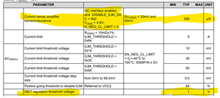
2. Furthermore, the CDC pin serves dual purposes: compensating for cable voltage drops and facilitating current sensing. Considering that the I2C interface is unused, what is its default operational role?
  • Moreover, if the CDC pin is functioning as a current monitoring device,should R(CDC) be determined using the equation V(CDC) = [V(ISNSP) - V(ISNSN)] × gm(CDC) × R(CDC) ?
Please kindly check whether the following parameter values are correctly assigned.
V(CDC) = 1 ? gm(CDC) = 500uS? [V(ISNSP) - V(ISNSN)] = R(ISNS) * Iout(max) ?Iout(Max)=6A or  Higher current value?
  • When employing the CDC pin for cable drop compensation, what is the suitable resistor value to be connected?
3. If the CDC is used for current sensing, is it still necessary to utilize the ILIMCOMP pin for detection purposes?With the I2C interface disabled, is it impermissible to employ an RC (resistor-capacitor) configuration for  the pin? How should this pin be handled?
 4. If utilizing ILIMCOMP for current sensing, the following formula must be employed:
V(ILIMCOMP) = [V(ISNSP) - V(ISNSN)] × gm(ILIMCOMP) × R(ILMCOMP) 
Please help provide the values for V(ILIMCOMP) and gm(ILIMCOMP).
Best wishes.
  • Hi Xiaoshan,

    thank you for using the E2E forum.


    Could you please attach the filled out LM51772 Design Calculator to this thread? This would be the most efficient workflow for us to do a schematic review.
     

    Best regards,

     Stefan

  • LM51772 Buck-Boost Quickstart Tool V1_1_1_副本.xlsm

    Hi,

    Please kindly find Attached file: LM51772 Design Calculator. Some parameters in the excel spreadsheet may be unsuitable.

    For instance, the information contained in the picture below is not entirely clear to me; Please kindly review it and simultaneously respond to the questions I have previously posed.

    Thank you very much!

  • Hi Xiaoshan,

    Thank you for the updated excel sheet.

    Please see my comments below

    1.

    Re-check items marked with bold:

    • Checked with Quickstart Calculator
       
    • Rcs in series with inductor and before inductor
    • Check filter for Rcs
    • Add filter cap between ISNSP and ISNSN  (placeholder)
    • Snubber on SW1 and SW2
      Place Footprint for a snubber at SW1 and SW2
       (they can then be populated in case needed (e.g. due to EMI) without layout change)
      Note: Snubber connect Resistor to GND for better Thermal performance
    • BIAS connected
      If BIAS is not used connect to GND or VIN of VOUT (do not keep open)
    • Add Series Resistor into MOSFET Gate signals lines
      (they can then be replaced in case needed (e.g. due to EMI) without layout change,
      additional option: add a diode in parallel for slow on and fast off.
    • Do not add resistor between SWx pin and Switch node
    • Voltage rating of MOSFET
      (Have a margin of 30% is recommended)
    • Miller Plateau of MOSFETs
      used MOSFETs need to be logic level MOSFETs - can be seen by Miller Plateau in the range of 2.5V-3.5V
    • UVLO setting relative to lowest input voltage
      UVLO is set to 8.7V but operating range starts at 12V - relative large distance


    • Cap at VCC 22uF : (Datasheet min: 10uF with DC Bias)
      please check the cap on Vcc to have the required capacitance considering DC BIAS - we use a 47uF on the EVM
    • VCC2 is for control and driver supply
      VCC1 can used for external logic - if not used can be disabled
    • Feedback divider identical for FB and FBIN (check if FBIN is required)
      FB_IN required: for pass through mode - only with external FB divider. With internal FB (FB connected to VCC2) put this to AGND
    • Connect FB to VCC2 if voltage should be set via I2C
    • nRST if not used needs to be connected to VIN

    Review Q7 : D_1 - it shows VOUT_FB which seems wrong

    Losses of >3W at BOOST Low side MOSFET will be hard to control from thermal perspective -> additional cooling required

    Losses of >2W at BUCK high side MOSFET will be hard to control from thermal perspective -> additional cooling required

    2.

    CDC used for Monitoring (default when I2C is disabled) : Yes, this formula should be used.

    3.

    if only the monitor is used (at CDC) then connect ILIMCMP to AGND 

    4.

    please use ILIMCMP for current limiting function and CDC for current monitoring

    Best regards,

     Stefan

  • HI,

     If utilizing ILIMCOMP for current limiting, the following formula must be employed:

    V(ILIMCOMP) = [V(ISNSP) - V(ISNSN)] × gm(ILIMCOMP) × R(ILMCOMP) 
    Please help provide the values for  V(ILIMCOMP) and  gm(ILIMCOMP).
    Thanks.
  • Hi Xiaoshan,

    please see the marked lines from the datasheet:

    Best regards,

     Stefan

  • HI,

    In both equations below:

    • V(ILIMCOMP) = [V(ISNSP) - V(ISNSN)] × gm(ILIMCOMP) × R(ILMCOMP)  
    • V(CDC) = [V(ISNSP) - V(ISNSN)] × gm(CDC) × R(CDC)

    V(ILIMCOMP) = V(CDC) = 1V, and gm(ILIMCOMP) = gm(CDC), therefore, R(CDC) should have the same resistance value as R(ILIMCOMP), right?

    I also have another question: Is it appropriate to set the value of I(ISNS) equal to Iout(MAX) = 6A?

    Thank you very much!

  • Hi Xiaoshan,

    Right for that both will have the same resistance.

    Yes, this can for sure be done. So you would limit the output current the the max current you have used for the design of the power stage.

    Best regards,

     Stefan