This thread has been locked.

If you have a related question, please click the "Ask a related question" button in the top right corner. The newly created question will be automatically linked to this question.

UCC28180: Regarding the distorted supply side current waveform.

Part Number: UCC28180
Other Parts Discussed in Thread: UC2854B

Dear Sir,

We are developing a boost-PFC converter. For the generation of the switching pulses currently we are using the UCC28180.

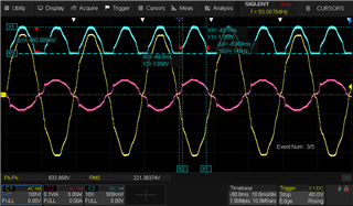
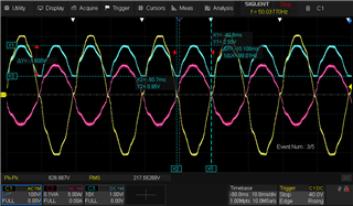
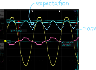
While experimenting for a power level of 1600W, we are getting distortion in the supply side current.

These distortion is getting worst in low power range.

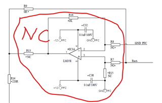
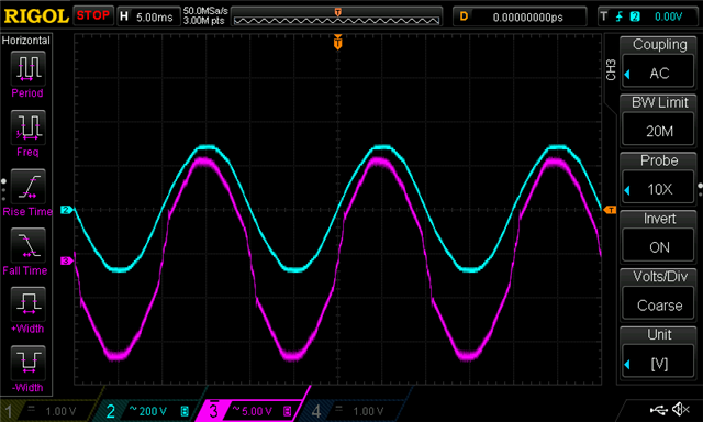
For your reference we are attaching the waveforms taken at the power level of 400W, 800W, and 1600W along with the PCB schematics.   
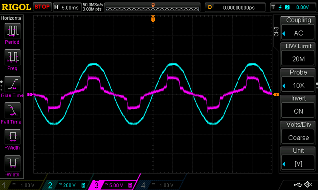
PFC BOARD RND 0.00 SCH.pdf

The values for the Experimentations are as follows:

Supply Voltage = 230V,

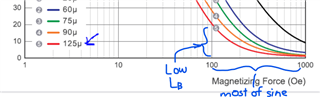
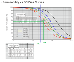
Boost Inductor  = 350uH,

Output Capacitor = 14 * 150uF = 2100 uF.

R sence = 10 mohm.

Switching Frequency = 100 kHz.

Please go through our query and give us a possible solution to get better supply current THD and UPF operation.

  • Hello SMPL, 

    I agree, the current waveforms are definitely distorted, and in an unusual way.  
    I see that the current waveform is shown on a 5V/div scale.  How is the this current being probed, and where is the probe located? 
    What is the conversion from V to A, please? 

    The AC voltage is shown at 200V/div, and the peaks look like ~300V (not sure exactly)   230Vac input has peaks to 325V, so either you are losing almost 25V between the AC source and the PFC input or actual input voltage is less than 230Vac.  This seems like a digression from the issue, but I want to be sure of what the peak current should be for a known input voltage and accounting for conversion losses.  

    In the schematic diagram, your VSENSE divider values program Vout = 443V.  Is this intentional?  If not, what Vout do you require? 
    What is the full required input voltage range for your PFC (such as 170Vac to 265Vac, or other range) and maximum Pout required? 

    Does your schematic accurately reflect the actual values of all the components shown, or have any of them been changed on the board being tested?
    There are several improvements to your PFC circuit that I can identify, but none of them pertain to THDi so I will refrain from discussing them until after the main problem is solved. 

    Can you please describe the type of boost inductor used here?  Is it made with a gapped-ferrite core or with powdered metal?  If powdered, what is the L vs. I curve, please?
    Is it possible to insert a current probe to measure the inductor current directly?  

    I'm looking forward to your replies.  I know I asked many questions.  For better support, please don't forget to answer all of them.

    Regards,
    Ulrich

  • Dear Ulrich,

    Thank you for your quick reply.

    Let me first Clarify you about your queries.

    1. The Current waveform is measured using a Current Probe of 10x Attenuation. We connected a EMI Filter before PFC. The Probe was located at the Phase Line at input of EMI Filter.

    2. The input AC Supply was provided from a Auto Transformer. I am attaching new measurements today where measurements are done at 230V.

    3. The Vout is required is 400V. We do not wish to boost upto 432V. Based on measured Vout our Engineer calibrated the divider.

    4. We have plan to use this design in different applications 

         400W : Line 85-270V

         800W :Line 85-270V

        1600W : Line 170-270V.

    Currently we are focusing on 1600W Design. We have been using our PFC using UC2854B IC, and we get satisfactory results.  Now we wish to reduce component count and cost. The PCB design is almost similar. We are getting very good THD in that Board. The board is being used in our production. So I am unable to share the gerber in forum but I can share it to your email if required.

    5. We are using Powder Iron Core Inductor. 

    Manufacturer : POCO

    Core PN:NPS250125

    Before Coating:OD×ID×HT=62×32.6×25 mm

    After Coating:OD×ID×HT=63.09×31.37×26.26 mm

    AL Value:400 nH

    Path Length:14.370 cm

    Ae:3.675 cm×cm

    Core Volume:52.81CC

    Inductor is designed with 29T with 34SWGx84 Wires Parallel. Inductance = 336uH

    Below is the DC bias graph

    Please find the attached file with More Measurements on 800W and 1600W Design. We have measured Inductor Current directly.

    Please note we changed out shunt value to 1 miliOhm to improve current Waveforms.

    ------------------------------------------------------------------------------------------------------------------------------------------------------------------------------------------------------

    The measurement results are attached in the following File.

    UC28180.docx

    Updated Schematics with the current test setup

    PFC Board_RND_0.00_PS

    PFC Board_RND_0.00 SCH

    Looking for your valuable feedback.

    SMPL Team

  • Hello SMPL Team, 

    Thank you for the additional information and waveforms.

    I believe that the main cause of distorted current is the boost inductor design. It is dropping to extremely low inductance at low bias current. 


    For powered-iron toroidal cores, H (Oe) = 0.4pi*mu*NI/le.  For your NPS250125 core, N=29, mu = 125, le = 14.37cm, and 1A drives H to = 101 Oe. 
    1600W out = ~1650Win = 7.17Arms = 10.15Apk line current.  So 10Apk will drive H to ~1000 Oe which drops mu to about ~2% of nominal.
    Most of the expected input "sine" current will operate between 1A and 10Apk, where boost inductance Lb is < 67uH down to about ~6.7uH at the peak!

    At very low Lb, the pk-pk ripple current is much larger than normal and the capacitor on ICOMP pin cannot filter the ripple adequately.  
    Also if the 2.5X current amplifier on ISENSE clips its output at the high input ripple peaks, then ICOMP will become distorted and affect the PWM generation adversely.  That is why the line current starts with a low amplitude at the zero-crossing and suddenly increases to a high amplitude where the current increases through the ~1A level.  Even at relatively low power (~400W) because the line current moves above 1A ( H > 100 Oe).   

    For better swinging-choke performance, the H-field needs to be confined to less than ~100 Oe at 10Apk.  
    From the equation, we see that to accomplish this mu and N must be lower, while le must be higher. 

    This will result in a much larger inductor.  Some compromise may be made to allow H = ~150 Oe at 10Apk.  
    But be aware that the 10Apk is the peak of the line frequency current at 230Vac.  
    This peak will be higher at 170Vac, but maybe THDi is not important there. 
    Also, the high switching frequency ripple pk is added on top of the line-freq peak, so Lb continues to reduce with the switching ripple amplitude. 

    Several design iterations and evaluations may be necessary to find the smallest inductor design to meet your THDi requirements. 

    Regards,
    Ulrich

  • Dear Ulrich,

    The formula you have used for Calculating H field should not contain mu in it. 

    The manufacturer software also calculates the inductance around 194 uH at 14A Peak. The dc bias graph also predicts similar. Also the current amplifier is disconnected and we are taking current feedback directly from shunt. (R8,R7 ,R13 is not populated and R9 = 0R and R14 = 220R)

    Core PN:NPS250125
    Core Number:1
    Frequency:100 kHz
    RMS Current:10 A
    Peak Current:14.14 A
    Ripple Current:2.828A
    Wire:1.8mm×2Pcs
    Turns:29
    Availabe Core Window Area::19.0934%
    Current Density:1.96 A/mm^2
    DCR:9.09mO
    ================================================
    L@0A:336.4µH
    L@10.00A:230.88µH (H=25.36Oe)
    L@14.14A:194.00µH (H=35.86Oe)
    ================================================
    Core Loss:8.848194 W
    Copper Loss:0.909W

    Total Loss:9.757


  • Hello SMPL,

    Uli is out of office so he will respond by the end of the week when he returns. In the meantime, can you please clarify your question and exactly what you need?

    Regards,

    Jonathan Wong

  • Hello SMPL team, 

    You are correct, my formula for H should not have mu in it. I consulted a faulty reference. My mistake.  

    After looking at the boost inductor current waveforms again, it looks like there is a shift from DCM to CCM and vice-versa at the locations where the AC current abruptly increases and decreases.  

    Please examine the ICOMP signal when the DCM/CCM transitions occur.  ICOMP is the filtered output of the current amplifier and it feeds into the PWM comparator.  If the ICOMP wave-shape does not follow the input voltage shape, then that will translate into high distortion.

    Your original schematic shows C28 = 2700pF.  Make sure that cap is working properly, without significant reduction from DC-bias effect.

    In the previous WORD document, I noticed that there is a connection between R9 and R6 that does not appear on the schematic diagram. 
    Please check that out, if it is intentional or a mistake. 

    Regards,
    Ulrich

  • Ulrich,

    We found that is a PCB Mistake. We will cut the track. However since Rf and Cf are open in our case, only 2700pF Connected. We will measure ICOMP voltage and share it with you.

    Since this is a feedback pin, is it OK to probe it? Or we should buffer it and check?

  • Hello SMPL Team, 

    Yes, it is okay to probe the ICOMP pin directly. 
    I recommend to use the "Tip & Barrel" method to avoid picking up switching noise which can obscure the signal.  

    Regards,
    Ulrich

  • Hello SMPL Team, 

    It has been over 3 weeks since your last posting. 
    Have you solved your problem?  
    If so, please let me know so I can close this thread. 

    Regards,
    Ulrich

  • Dear Ulrich,

    After all the suggestion and implementations, the current distortion is still present.

    Regards,

    SMPL Team

  • Hello SMPL Team, 

    I was waiting for you to provide ICOMP waveforms that correspond to the different ac current distortions at different line and load conditions.  
    Your post of May 6th indicated that you would measure ICOMP and share the waveforms.  

    Please use 1ms/div sweep and 0.5V/div for ICOMP, 100V/div for rectified input RECT+, 2A/div for AC input current. 
    Place the zero-references on the same horizontal graticule line.  Focus on the zero-crossing region.

    Regards,
    Ulrich

  • Hello,

    We have tried to measure waveforms on the ICOMP pin but have faced a few problems:

    1. Tried to measure the waveform directly with a probe in the "Tip & Barrel" method (as suggested).

        Result: The input (AC) line fuse (rated at 6A) burned at an output voltage of 50Vdc (without load).   

    2. Tried to measure the waveform by using an opamp (in Unity gain buffer mode with 10Kohm resistor in series).

        Result: PFC didn't boost the voltage.

    3. Tried to measure the waveform by using an opamp (in Unity gain buffer mode without any series resistor).

        Result: The input (AC) line fuse (rated at 6A) burned at an output voltage of 50Vdc (without load).

    Supply Voltage: 230Vac, 50Hz

    Required Output Voltage: 400Vdc

  • Hello SMPL Team, 

    The symptoms you describe as a result of probing the controller strongly indicate that your AC source is not isolated.  

    The oscilloscope probe ground is connected to the 'scope chassis ground which is directly connected to earth-ground through the line cord.
    If you are powering your PFC directly from the building AC outlet or through a non-isolated variable transformer (such as Variac), then the 'scope GND will short out the AC input through the PFC diode bridge and, in the best case, blow the fuse.  Often the diode bridge is also damaged.    

    You cannot safely probe the primary side of any converter (PFC or otherwise) unless you are using an isolating probe OR the AC source is isolated.
    In my experience, HV isolating probes distort low level signals, so I always use normal X1 and X10 probes for debugging and use an isolated AC source to power the circuit.  Whatever node the probe GND is connected to will assume earth-GND potential.  

    AC power can be sourced from an electronic AC supply (with input to output isolation) or using a  50Hz 1:1 isolation transformer between the wall outlet and the PFC input.  You must have the isolation. 
    And when probing several signals at once, the probe GNDs must all be connected to the same reference node.  You can't have two different reference GNDs or damage will result.  

    Regards,
    Ulrich

  • Hello Ulrich,

    Thanks for your advice to keep the isolation. 

    Here, I have attached the waveforms for 400Watt, 800Watt and 1600Watt.

    Channel 1: Input Voltage (230VAC, 50hz).

    Channel 2: Input Current.

    Channel 3: Voltage measured at ICOMP pin.

    1. For 400Watt:

    2. For 800Watt:


    3. For 1600Watt:

    Regards,

    SMPL Team

  • Hello SMPL Team, 

    Thank you for the ICOMP waveforms.  They are not usual, in the sense that normally, the ICOMP signal more closely resembles a rectified sine current with valleys near the zero-crossings.  

    Instead, these ICOMPs seem to have a DC "floor" level of about 1V or higher.  
    The "floor" seems to correspond to areas where the inductor current may be operating in DCM instead of CCM. 
    Lighter load has more DCM and higher "floor" voltage.

    For an experiment, please connect two inductors in series to see if the higher inductance lowers the "floor" voltage. 
    I do expect higher L to reduce the amount of DCM operation for the same output power levels (400, 800, 1600W).  

    While you have the 2nd inductor installed, may I also request a screen capture of a single switching cycle of inductor current taken at the peak of 230Vac input with 1600W output, please?   

    Regards,
    Ulrich

  • Hello Ulrich,

    We have DOUBLED the inductor value but still facing the same issue.

    Here, I have attached the waveforms for 400Watt, 800Watt and 1600Watt.

    Channel 1: Input Voltage (230VAC, 50hz).

    Channel 2: Input Current.

    Channel 3: Voltage measured at ICOMP pin.

    1. For 400Watt:

    2. For 800Watt:

    3. For 1600Watt:

    Regards,

    SMPL Team

  • Hello SMPL Team, 

    There is a very slight reduction in the "DC floor" level in each screen shot, but I'm not sure why or if it is significant. 

    But I do think that the cause of the DC level factors heavily into the poor THDi. 
    I don't have an answer yet and have to think more about this. 

    Can you please provide an updated copy of the schematic diagram, as your circuit is implemented today? 
    I would like to be sure that I am working with the latest and correct information. 

    Regards,
    Ulrich 

  • Hello Ulrich,

    Sorry for the late reply.

    We are using the same Schematic, provided before.

    [Schematic: PFC BOARD RND 0.00 SCH (2).pdf]

    This time we have changed the inductor value only.

    Regards,

    SMPL Team

  • Hello SMPL Team, 

    Thank you for resending the schematic file.  I am glad that nothing has changed (except for the inductance). 

    At this time, I can think of only one possibility for the "DC floor" voltage on ICOMP: I suspect some negative input offset voltage on ISENSE. 
    The schematic diagram indicates that several components on ISENSE are not connected (NC) and should not cause any issue.

    But I request that you please verify that your board is actually depopulated according to the schematic.
    In fact, I request that you please remove all of the parts that are encircled, even if you are certain that R13 is not loaded.

    Also, please remove D4 from your board as well, and verify that C29 is 1nF and R14 is 220 ohm, not some unwanted values. 

    I wish to eliminate the possibility that anything is affecting the ISENSE signal from R1 (10mR) except the R14-C29 filter. 
    And please verify that the "GND_PFC" net on the controller page of the schematic is directly connected to the "PFC_GND" net on the power stage page of the schematic.  

    I probably should have though to ask this a long time ago:  Have you tried replacing the UCC28180 IC with a new one? 
    I ask in case there is some permanent damage done to the IC due to ESD or board-debug probing error or something.  

    Regards,
    Ulrich