This thread has been locked.

If you have a related question, please click the "Ask a related question" button in the top right corner. The newly created question will be automatically linked to this question.

TPS7B7702-Q1: Need to confirm the RJa data using the standard board.

Part Number: TPS7B7702-Q1

Hi Team,

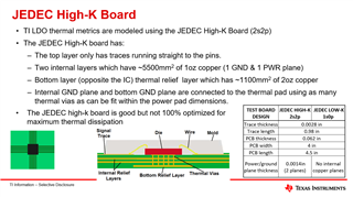
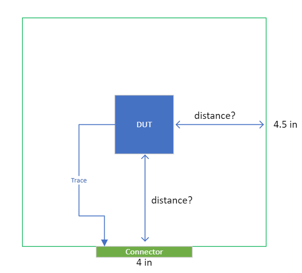
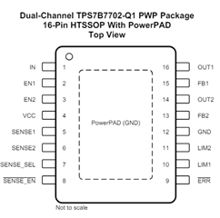
We are using the TPS7B7702-Q1, we are very care about the Rja data, the application is the automotive. So we plan to design a resistance test board to double-confirm the Rja data just like datasheet said, to make sure and select the qualified device, Rja should be about 40.3℃/W.

But we don't have the detailed requirement for the below JEDEC standard, and if you can share it to us or show the reference Rja test board, will be appreciate, thanks in advance.

Best Regards,

Kunyue

  • Hi Kunyue,

    See the attached image for information on the JEDEC High-k board layout used to simulate the thermal metrics. Please let me know if it is not clear. 

    Regards,

    Nick

  • Hi Nick,

    Thank you so much for your detailed sharing. I still have some questions about this board.

    1, We should place the DUT in the middle of board?

    2, The trace length is only 0.98 in, so how to connect it to the connector?

    3, We need to make sure the second layer is the PWR, and the third layer is the GND? Right? What is the PWR mean? Just like the TPS7B7702-Q1, the PWR is mean the VIN? Or VOUT? If it has the two VOUT, we need to connect them together?

    4, For the ''thermal vias'', how many vias I need to add? 

    Thanks in advance.

    Best Regards,

    Kunyue

  • Hi Kunyue,

    1, We should place the DUT in the middle of board?

    Yes the DUT is in the middle of the board.

    2, The trace length is only 0.98 in, so how to connect it to the connector?

    This JEDEC board is only for simulation purposes to evaluate thermal performance so there is no connector at the edge of the board. The traces simply terminate at the edge of the board. 

    3, We need to make sure the second layer is the PWR, and the third layer is the GND? Right? What is the PWR mean? Just like the TPS7B7702-Q1, the PWR is mean the VIN? Or VOUT? If it has the two VOUT, we need to connect them together?

    Not necessarily. The purpose of this is to provide metrics for thermal performance with a known PCB layout. If your board has a similar amount of copper as the JEDEC board, then you can expect similar performance to the metrics reported in the datasheet. Your layout does not need to match the JEDEC board, and usually won't. In many cases PCBs use more than 4 layers, and also have more than one GND layer, which helps to improve the thermal performance.

    PWR in this case is short for "power", i.e. a plane dedicated mostly to distributing power to the various circuits. On a real board this layer would probably be used to route the VIN and VOUT nets (not connected together). They are included in the JEDEC board because even though they do not directly conduct heat through metal, they do provide more thermal mass.

    4, For the ''thermal vias'', how many vias I need to add? 

    In general it is advised to fit as many minimum-sized vias under the thermal pad. The minimum size depends on the board manufacturer. For example, cheaper board fabrication processes may support 10mil minimum drill size, and other board manufacturers can support 4mil hole size for standard board fabrications or even smaller for more advanced board fabrications. Whatever the minimum drill hole size is for the board manufacturer you will use, fit as many minimum-sized vias under the thermal pad that comply with the spacing requirements of the board manufacturer.

    Regards,

    Nick

  • Hi Nick,

    Thank you so much, your explain are so clear, I am clear now.

    Best Regards,

    Kunyue