Because of the holidays, TI E2E™ design support forum responses will be delayed from Dec. 25 through Jan. 2. Thank you for your patience.

This thread has been locked.

If you have a related question, please click the "Ask a related question" button in the top right corner. The newly created question will be automatically linked to this question.

LM5123-Q1: Please review this boost converter design

Part Number: LM5123-Q1

Respected TI experts

I kindly ask you to review the component selection and the layout of this boost converter design.

For context: this is an LED driver working up from a 5S2P li-ion battery pack. (Current) regulation is done via the tracking input with an external MCU and current sense resistor. There is also an external low-side switch to quickly turn the LED on or off (strobe functionality).

The converter is intended to be functional with full power output of 3.2A@54V at 17.5V minimum input.

To minimize switching losses in this thermally challenged application (there is only a little airflow from a nearby cooling fan), a relatively low switching frequency of about 120KHz was selected.

Because the inductor would otherwise be huge, expensive and poorly available, a high ripple current ratio of about 60% had to be chosen. I accept the resulting higher core loss and lower light load efficiency (earlier DCM).

The PCB is a 6-layer board with plated-over filled vias and 1-0.5-0.5-0.5-0.5-1 oz copper thickness. 6 layers are used because they are needed for other parts of the application.

My primary concerns are:

  1. Do you advise against using a current sense resistor value smaller than recommended by the quickstart calculator? As I see it, it will reduce losses and low frequency gain. The current limit would also be too high, but that is already taken care of by the battery protection circuitry. Would 2mΩ or even 1mΩ be fine too?
  2. Is the QH-QL-COUT loop small enough? Does it need more small output capacitors? Currently there are two 0805 100nF X7R output capacitors directly besides QH and one near the device.
  3. The RS-LM-CIN loop is not as critical (less di/dt) but is it fine too?
  4. Is SW/HO/Vout routed directly enough? The "accessory" capacitors are somewhat in the way, but I'd like to not have to use smaller packages with poor DC bias characteristics.
  5. Is LO/GNDPWR routed directly enough? LO is wide and runs on the GNDPWR plane but has vias in the way.
  6. I surrounded the rather long current sense tracks with GNDA zones above and below. Is this a bad idea?
  7. The SW pour is on the smaller side. I believe that the massive copper wire of the inductor will sink away some of the heat and a large noisy plane for heat dissipation is therefore not necessary.

EDIT: All attachments have been removed from this question as they were reported to be missing!

Thank you very much in advance,

Adrian

  • Hello Alan,

    Thanks for reaching out to us via e2e.

    First of all: I cannot see open any of your attachments.
    Drag & Drop does not work in this forum. Please use the Insert Image/video/file function to add content.

    Let me answer some of your questions upfront.

    A properly sized sense resistor is very important, as it is not just meant as an overcurrent protection.
    The current sense controls the inner cycle-by-cycle regulation loop. Therefore, the fundamental control loop will not work when the sense resistor is too small.

    Surrounding the current sense tracks with GNDA zones above, below and around them is actually a good idea.
    This is true for all sensitive signals (those that are connected to AGND).
    For a six-layer stack, I would propose the following setup:

    Power Stage, PGND (at least underneath the power stage area), AGND as shield, sensitive signals, AGND as shield, less sensitive signals

    Use a separate AGND Polygon for the signals that are connected to AGND.
    As described in the datasheet, the only connection between AGND and PGND should be via the exposed pad of the controller.

    Generally, the switch node polygon should be kept as small as possible (knowing that the low-side FET will maybe need this polygon for cooling.

    I am a bit worried about the external low-side switch for the strobe functionality that you have mentioned.
    I will comment on it, as soon as I can see the schematic.

    All information in this correspondence and in any related correspondence is provided “AS IS” and “with all faults” and is subject to TI’s Important Notice (www.ti.com/.../important-notice.shtml).

    Best regards
    Harry

  • Hello Harry

    Thank you for your swift answer!

    Please excuse the missing attachments. Strangely I can see all the images, even logged out on a different browser... The images and the filled calculator are attached to this reply as a zip archive. Hopefully this works.

    About the sense resistor: thank you for the hint, I will leave it exactly as recommended by the quickstart calculator (rounded to 1mΩ). Although I do not know the best value for the current limit margin, which determines the calculated value. Do you think the 3mΩ are fine? This is the recommended value for a margin of 60%.

    The current layer stack-up does not reflect your recommendation. It uses multiple layers for high current zones to minimize resistance and impedance. What do you think of it? It seems to me that Power and Signal are well separated, but I might be mistaken. 

    A net-tie is placed to connect PGND and AGND at the exposed pad.

    The size of the SW pour is difficult to judge without an image ;-)

    One image is an extract from the schematic on which the external low-side strobe FET is located. Do you worry about the hight di/dt transient it introduces? If necessary, the slew rate can be limited via RC smoothing.

    I'm looking forward to your response.

    Best regards,
    Adrian

    TI_E2E_LM5123-Q1_Layout_Review_Attachments.zip


  • Hello Adrian,

    Thanks for the files.

    There is a lot of room for improvement, already in the schematics.
    It is missing most of the important components. What did you use as a reference?
    Please have a look at our EVM which shows the necessary parts.

    - A DC/DC converter cannot work without ceramic input /output capacitors of a reasonable size.
    You will need to add multiple 10 µF ceramic capacitors on the output.
    Place one of the 100 nF and 10 uF caps very close to the high side FET.
    - Please add placeholders for gate resistors (in the gate lines).
    The LM5123 is actually designed for Dual FETs. With single FETs, you will need to add gate resistors in the range between 2 Ohm and 5 Ohm.
    Please make sure that you will keep both resistors the same and also do not go above 5 Ohm.
    - Please add the filter for the current sense signal.
    Do NOT insert a resistor in the CSP line !
    But insert a resistor in the CSN line and a cap between CSP and CSN. Place this capacitor as close to the controller as possible.

    The low-side FET is the one that will dissipate most of the heat.
    It is counterproductive if this FET is using a small package.

    For the layout, please follow the Layout Guidelines in chapter 11 in the datasheet.
    In the example that is shown in Figure 11-1, the power stage has a U-shape (input and output on the left side).
    This placement is much better than the one you will see on the EVM (left to right).
    If possible, follow such a U-shape.

    The optimal placement for the gate loops is on top of each other, on adjacent layers.
    If you want to use this placement, method (instead of side by side on the same layer), please make sure that the tracks are on directly adjacent layers with nothing in-between.
    LO directly above PGND (to the PGND pin). And HO directly above SW,

    The shields for the sensitive signals are principally a good idea, but they need to be much wider (sticking out beside the signal tracks).
    But please, do never leave and tracks floating on one end, especially not those that are meant for shielding.
    Such tracks will form antennas and pick up a lot of noise.
    Either use complete AGND layers to shield the sensitive signals, or at least some big, connected areas.

    By the way, are the black areas really free of copper?
    Please talk to your board vendor if this is a good idea.
    I heard that such un-even distribution of copper will make the board unstable.

    All information in this correspondence and in any related correspondence is provided “as is” and “with all faults” and is subject to TI’s Important Notice (http://www.ti.com/corp/docs/legal/important-notice.shtml).

    Best regards
    Harry

  • Hello Harry,

    Thank you for reviewing the first revision and your detailed recommendations!

    There is a lot of room for improvement, already in the schematics.
    It is missing most of the important components. What did you use as a reference?
    Please have a look at our EVM which shows the necessary parts.

    In this case, I'm glad I asked. This is my first time designing a higher-power switching power supply, and it shows... :-)
    To answer your question: I used the datasheet of the LM5123-Q1 and this application note. I also looked at the EVM's schematic, but admittedly I just glanced at its layout. For the layout I followed the Layout Guidelines section of the datasheet.

    About your recommendations:

    You will need to add multiple 10 µF ceramic capacitors on the output.

    I believe a note in the datasheet would be helpful. When I saw them on the EVM I thought they were there just to minimize ripple.

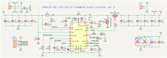
    Revision 2 has four 10µF 1210 X7S output capacitors. I added two on the input too. Please tell me if you think more would be beneficial.

    Is it correct that using too few medium-value (10µF) ceramic output capacitance (as in revision 1) not only means higher output ripple but also destabilizes the control loop, even though there are high-frequency (100nF) filtering capacitors?

    Are the electrolytic capacitors mainly there to provide better transient performance or do they significantly affect the control loop? If they aren't critical for stability, their number could be reduced or smaller values chosen to save cost and space.

    Please add placeholders for gate resistors (in the gate lines).

    I assume this is to prevent potential ringing at the gate with such a small gate charge.
    Do you think it is much preferable to have two FETs for this design? Total conduction losses would be halved. From my undestanding, total switching losses would double due to rise/fall time degradation caused by the doubled gate charge. Is this true?

    Please add the filter for the current sense signal.

    It is described in the datasheet as an "optional component", why?
    The EVM uses values of 100pF and 100Ω. Are these general values suitable for this design as well?

    The low-side FET is the one that will dissipate most of the heat.
    It is counterproductive if this FET is using a small package.

    Thank you for the hint, but this model should be used to deplete our stock.

    For the layout, please follow the Layout Guidelines in chapter 11 in the datasheet.
    In the example that is shown in Figure 11-1, the power stage has a U-shape (input and output on the left side).
    This placement is much better than the one you will see on the EVM (left to right).
    If possible, follow such a U-shape.

    Wasn't revision 1 already following such an U-shape?

    The optimal placement for the gate loops is on top of each other, on adjacent layers.
    If you want to use this placement, method (instead of side by side on the same layer), please make sure that the tracks are on directly adjacent layers with nothing in-between.
    LO directly above PGND (to the PGND pin). And HO directly above SW,

    For revision 2, the gate and source traces run mostly on top of each other to minimize loop area. Please see the new images. The gate resistors are somewhat in the way though: I question that the proximity of the HO trace (blue) to the SW trace (brown) makes up for the two vias. Consider this alternative route (pink):

    The shields for the sensitive signals are principally a good idea, but they need to be much wider (sticking out beside the signal tracks).
    But please, do never leave and tracks floating on one end, especially not those that are meant for shielding.
    Such tracks will form antennas and pick up a lot of noise.
    Either use complete AGND layers to shield the sensitive signals, or at least some big, connected areas.

    Revision 2 uses layer 5 for a complete AGND shielding and reference plane. The current sense traces are routed on the bottom layer.

    By the way, are the black areas really free of copper?
    Please talk to your board vendor if this is a good idea.
    I heard that such un-even distribution of copper will make the board unstable.

    They say it is fine, but I changed it to a more even distribution anyway.

    Some other questions:

    1. What about the external strobe FET?
    2. In the datasheet's example layout, PGND has a slit separating the zone (see the image). On the EVM such a gap is not present, but it has a significantly different layout anyway. Do you recommend this?

    Hopefully the images are correctly inserted this time:

    Schematic rev. 2:

    PCB layers rev. 2, 3D then top to bottom:

    Just in case, I again include a zip archive:

    Images_Revision_2.zip

    Best regards,
    Adrian

  • Hello Adrian,

    The expert for this device is out of the office until beginning of next week. Expect an answer from him beginning of next week.

    Most important is that you know exactly where the current of the power stage is flowing when the power switch is on and when the sync FET is on. And have a look at the return path as well. You should always start at the input capacitor and then follow the current loop and get back to this input capacitor. Next important are the gate signals of the MOSFETs. Keep them short and if possible on top of each other and do not forget that SW is the return for the high-side FET.

    Best regards,
    Brigitte

  • Hello Brigitte,

    Thank you for the information.

    Yes, I paid attention to the current loops and tried to follow all of Harry's recommendations. I'm looking forward to his opinion of revision 2.

    Best regards,
    Adrian

  • Hello Adrian,

    This looks much better now.
    I would completely remove C9 and only keep C8 next to the FET (maybe move C9 close to J2).
    This will give you a more direct connection in the PGND layers.
    Can you build an AGND island on the top layer (as shown in the datasheet)?
    Then all the AGND components will be connected more directly rather than through all these VIAs.

    I'll have a closer look at more details of the gate loops and current sense signals later today.

    I am not so happy with the fact that you are cutting so much through the GND layer on the bottom layer.
    For thermal reasons it would be better to move the tracks to a inner layer between two AGND layers - or at least AGND sections.

    The gap in the GND plane is meant to "shield" the input from the more noisy output.

    Can you please describe the strobe concept in more detail:
    Do you want to completely disconnect the load an then turn it back on?
    Is it meant to be a digital function (completely on or off with no smooth transition between these two states?
    What is the timing (PWM frequency and duty cycle range)?

    Why are you using two different FETs (high-side vs. low-side)?


    Best regards
    Harry

  • Hello Harry,

    Thank you very much for your reply!

    I would completely remove C9 and only keep C8 next to the FET (maybe move C9 close to J2).

    C9 has been moved near J2.

    Can you build an AGND island on the top layer (as shown in the datasheet)?
    Then all the AGND components will be connected more directly rather than through all these VIAs.

    An AGND island has been established. I left the vias there to ensure good connection to the other AGND planes.

    I am not so happy with the fact that you are cutting so much through the GND layer on the bottom layer.
    For thermal reasons it would be better to move the tracks to a inner layer between two AGND layers - or at least AGND sections.

    I assume the worst offender is the Vout trace since it runs below the hot switches? Its route has been modified, however it is not on an inner layer as you suggested. Do you think this mostly alleviates the negative thermal effect?

    The gap in the GND plane is meant to "shield" the input from the more noisy output.

    The input is noise insensitive. It seems to me that a gap would just increase resistance. Do you recommend it?

    Can you please describe the strobe concept in more detail:
    Do you want to completely disconnect the load an then turn it back on?
    Is it meant to be a digital function (completely on or off with no smooth transition between these two states?
    What is the timing (PWM frequency and duty cycle range)?

    Yes, it is a full disconnect and purely on or off. The plan is to implement a strobe/blinking effect. It is not meant to dim the LED by means of PWM, the LM5123-Q1's output voltage tracking is used for this purpose. The maximum frequency would be below 50Hz. The duty cycle could range from 0% to 100%.
    The special case of 0% duty cycle will be used to completely disconnect the LED from the battery pack when the device is off.
    The slew rate of the external FET can be reduced if the transients turned out to be generating too much EMI.

    Why are you using two different FETs (high-side vs. low-side)?

    The low-side FET has a lower gate charge. The high-side FET has a lower reverse recovery charge.


    The schematic has not changed from revision 2. Here are the PCB images for revision 3, 3D and top to bottom:

    Best regards,
    Adrian

    EDIT: I have added some vias to the new AGND island below the Booster_Enable track as to not have it float. The images do not show this.

  • Hi Adrian,

    Due to bank holiday, please expect a reply by Friday.

    Best Regards,

    Feng

  • Hello Feng,

    Thank you for the information.

    Best regards,
    Adrian

  • Hello Adrian,

    I am sorry for the additional delay.

    With regards to the gap in the GND area:
    Generally, the input is noise insensitive, but in applications like yours where you are turning the load on and off you may see some influence.
    Anyway, for now I would not say such a gap is necessary.

    The gate drivers of the LM5123 have been designed for Dual FETs. Connecting single FETs is already creating quite some ringing and you will need to add gate resistors to minimize that.
    Therefore, using a FET with a low gate charge will make the problem even bigger.
    Therefore, for thermal reasons and to allow for symmetry for the adaptive dead-time control, I would recommend using the high-side FET also for the low-side.

    Regarding the bottom layer I think I could not get the point across.
    The sense of the thermal VIAs underneath the controller is to guide the heat through the board to the bottom layer and to use that copper area on the outer layer as a heat spreader.
    But all the tracks on the bottom layer are basically cutting through that heat spreader and minimizing that solid copper area.
    So, for thermal reasons it would be better to move the tracks to an inner layer - between two AGND layers or at least AGND sections.

    CSN and CSP are very sensitive. Also the TRK signal is pretty sensitive and should be shielded from noisy (switching) signals.
    As you can imagine, PGOOD is unsensitive and can be routed anywhere.

    The switch node should be kept small. so please do NOT add a big polygon on the bottom.

    I would propose the following layer stack-up:

    Top layer: Power stage with PGND + AGND island
    Layer 2: Solid PGND layer + Vin and Vout polygons + gate drive signals
    Layer 3: Solid PGND layer
    Layer 4: Solid AGND layer as shield
    Layer 5: Solid AGND layer + sensitive signals
    Bot Layer: Solid AGND layer (cooling of the controller)
    Do NOT create a gap between AGND and PGND or any other signal underneath any of the sensitive signals in layer 5!

    I am still worried about that strobe concept.
    Quickly changing loads will force the controller to try to compensate for that.
    I doubt that you can increase the slew rate in a way that it will reach across multiple cycles of the booster.

    Maybe you can experiment with the TRK function to slowly turn down the output before you turn of the LEDs completely.

    All information in this correspondence and in any related correspondence is provided “AS IS” and “with all faults” and is subject to TI’s Important Notice (www.ti.com/.../important-notice.shtml).

    Best regards
    Harry

  • Hello Harry,

    Thank you for your reply!

    With regards to the gap in the GND area:
    Generally, the input is noise insensitive, but in applications like yours where you are turning the load on and off you may see some influence.
    Anyway, for now I would not say such a gap is necessary.

    OK, the gap has not been added for now.

    The gate drivers of the LM5123 have been designed for Dual FETs. Connecting single FETs is already creating quite some ringing and you will need to add gate resistors to minimize that.
    Therefore, using a FET with a low gate charge will make the problem even bigger.
    Therefore, for thermal reasons and to allow for symmetry for the adaptive dead-time control, I would recommend using the high-side FET also for the low-side.

    Both FETs are now the same model. My thought was to minimize switching loss by reducing gate charge, but I guess the ringing would not help either.

    Regarding the bottom layer I think I could not get the point across.
    The sense of the thermal VIAs underneath the controller is to guide the heat through the board to the bottom layer and to use that copper area on the outer layer as a heat spreader.
    But all the tracks on the bottom layer are basically cutting through that heat spreader and minimizing that solid copper area.
    So, for thermal reasons it would be better to move the tracks to an inner layer - between two AGND layers or at least AGND sections.

    Excuse me, I did not consider the thermals of the controller. I assumed its power dissipation to be small. There is no value given in the datasheet concerning the total power dissipation during operation, only sleep modes and the maximum the Vcc regulator can supply. What should be expected?

    The switch node should be kept small. so please do NOT add a big polygon on the bottom.

    Do you think the current zones for cooling (Vout and SW on the back layer) are too large? I believe they help FET thermals greatly.

    I would propose the following layer stack-up:

    Top layer: Power stage with PGND + AGND island
    Layer 2: Solid PGND layer + Vin and Vout polygons + gate drive signals
    Layer 3: Solid PGND layer
    Layer 4: Solid AGND layer as shield
    Layer 5: Solid AGND layer + sensitive signals
    Bot Layer: Solid AGND layer (cooling of the controller)

    The stack-up has been adjusted to suit your recommendation. Should layers 2 and 3 have the analog island too?

    Do NOT create a gap between AGND and PGND or any other signal underneath any of the sensitive signals in layer 5!

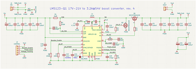
    What exactly do you mean? Do you mean that layer 4 and 6 should be solid AGND planes? Rev. 4 has gaps in these layers only for vias and THT pads. (And the two cooling zones plus MODE solder bridge on the back layer)

    I am still worried about that strobe concept.
    Quickly changing loads will force the controller to try to compensate for that.
    I doubt that you can increase the slew rate in a way that it will reach across multiple cycles of the booster.

    During characterization, are there any signals besides Vout and SW to be checked/probed to confirm safe behaviour during these strobe switching transients?

    Maybe you can experiment with the TRK function to slowly turn down the output before you turn of the LEDs completely.

    Great idea, we will try this for sure.

    Schematic of rev. 4:

    PCB images of rev. 4, 3D and top to bottom:

    Best regards,
    Adrian

  • Hello Adrian,

    You are right, the power dissipation of the controller is comparably small.
    Nevertheless, there is no polygon to be used as heat spreader on the top layer,
    Therefore, as the thermal VIAs exist, it will be better to at least allow for some dissipation on the bottom layer.

    There is no value given in the datasheet because it depends a lot on the external components.
    Vin and the voltage drop on the internal regulator are just one portion. In addition, you will see the power dissipation of the gate drivers, also when the gate pins get pulled to GND.

    The current zones for cooling (Vout and SW on the back layer) are not too large. I just mentioned it to avoid that you will make them bigger.

    Yes, layer 4 and 6 should be solid AGND planes, at least in the region where the sensitive signals are routed.
    Gaps due to vias and cooling areas are fine.

    An analog island on layer 2 is nice to have, as it will shield the signals on the top layer from below, Layer 3 does not need it.
    It is not really necessary to place that many VIAs along the border between AGND and PGND.

    There is one thing that should still be changed:
    The LO track in layer 2 is now placed directly underneath the border between AGND and PGND on the top layer.
    It should be covered by PGND only.

    Maybe move R6 and the track for the Enable signal further up.
    Then move the border of the AGND island on the top layer also further up to the region where all these VIAs are placed now.
    On layer 2 it would also be good if LO track could be completely surrounded by PGND (a thin PGND area between LO and the AGND island.

    For the bring-up:
    Besides Vout and SW it would be interesting to see the inductor current measured between R1 and L1 (lift the inductor and insert a cable loop for a current probe), as well as LO and HO.
    You will need to adjust the gate resistors, so that there are no over/undershoots / ringing on the switch node and the gate drive signals.

    > Maybe you can experiment with the TRK function to slowly turn down the output before you turn off the LEDs completely.
    similarly for the turn-on procedure: Start with a low TRK voltage, turn on the load, then increase the TRK voltage in multiple small steps, so that the power stage is able to follow.

    By the way, the datasheet says that UVLO/EN must not be higher than BIAS+0.3V.
    So, please do not drive the Enable signal high while Vin is not yet applied.

    Best regards
    Harry

  • Hello Harry,

    Thank you for your feedback. I believe this design is nearing the first prototype with revision 5.

    There is one thing that should still be changed:
    The LO track in layer 2 is now placed directly underneath the border between AGND and PGND on the top layer.
    It should be covered by PGND only.

    Maybe move R6 and the track for the Enable signal further up.
    Then move the border of the AGND island on the top layer also further up to the region where all these VIAs are placed now.
    On layer 2 it would also be good if LO track could be completely surrounded by PGND (a thin PGND area between LO and the AGND island.

    LO is now completely surrounded with PGND.

    For the bring-up:
    Besides Vout and SW it would be interesting to see the inductor current measured between R1 and L1 (lift the inductor and insert a cable loop for a current probe), as well as LO and HO.
    You will need to adjust the gate resistors, so that there are no over/undershoots / ringing on the switch node and the gate drive signals.

    With single FETs, you will need to add gate resistors in the range between 2 Ohm and 5 Ohm.
    Please make sure that you will keep both resistors the same and also do not go above 5 Ohm.

    I will keep 3Ω and 4Ω resistors ready to replace the 2Ω ones placed at first.

    Start with a low TRK voltage, turn on the load, then increase the TRK voltage in multiple small steps, so that the power stage is able to follow.

    TRK is fed from a 12-bit DAC with a voltage divider. This yields about 14mV of output voltage for every DAC bit. Voltage will be ramped one bit at a time.
    Do I understand correctly that adjusting TRK too quickly does not damage the controller, but may cause over- or undervoltage protection to trigger?

    By the way, the datasheet says that UVLO/EN must not be higher than BIAS+0.3V.
    So, please do not drive the Enable signal high while Vin is not yet applied.

    This is fortunately impossible because the MCU giving out the enable signal and the LM5123-Q1 are powered on at the same time.

    Revision 5 PCB images, 3D then top to bottom:

    Best regards,
    Adrian

  • Hi Adrian,

    Please expect a reply by tomorrow due to public holiday.

    Best Regards,

    Feng

  • Hello Feng,

    Thank you for the info.

    Best regards,
    Adrian

  • Hello Adrian,

    Yesterday was a public holiday for us and I am very busy right now.
    I will get back to you later today.

    All information in this correspondence and in any related correspondence is provided “AS IS” and “with all faults” and is subject to TI’s Important Notice (www.ti.com/.../important-notice.shtml).

    Best regards
    Harry

  • Hello Harry,

    No problem, take your time. I can wait a few days.

    Best regards,
    Adrian

  • Hello Adrian,

    Thanks for your patience.

    To me, the layout looks pretty good now.

    You may not need to ramp one bit at a time, you can take bigger steps.
    The LM5123 will only react at the beginning of a new cycle (switching frequency).

    You will need to run some experiments to see the reaction of your power stage.

    > ... adjusting TRK too quickly does not damage the controller, but may cause over- or undervoltage protection to trigger?
    Yes, this is the main concern.

    The conroller can be damaged if there are too big under-and overshoots, especially on the switch node and the gate driver outputs.
    So, please have a look at these signals during the bring-up.

    All information in this correspondence and in any related correspondence is provided “AS IS” and “with all faults” and is subject to TI’s Important Notice (www.ti.com/.../important-notice.shtml).

    Best regards
    Harry

  • Hello Harry,

    Thank you very much for your detailed insight and guidance!

    Best regards,
    Adrian