This thread has been locked.

If you have a related question, please click the "Ask a related question" button in the top right corner. The newly created question will be automatically linked to this question.

BQ76952: Low-side FET Control

Part Number: BQ76952
Other Parts Discussed in Thread: EV2400, BQSTUDIO

Hello TI Expert!

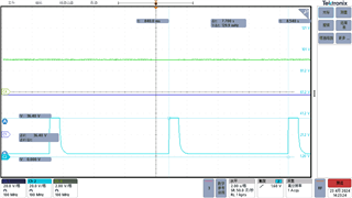
I used the Low-side FET to control the FET when using BQ76952. Now I have a problem I want to confirm. When BQ works in normal mode, I use STM32 to give a level (3.3V or 0V) to control the DFETOFF and CFETOFF pins, which work fine. After the BQ enters the shurdown mode, there is a probability that DHG will be on and off all the time when the DFETOFF and CFETOFF pins are tdown after being wake-down from the shurdown mode. Want to know what's causing this?
I look forward to your reply. Thank you!

  • Hello Zhang,

    I am confused exactly at what you are trying to explain. Can you provide me steps on your sequence? 

    If the part is in SHUTDOWN, the pins would have no voltage at all.

    Best Regards,

    Luis Hernandez Salomon

  • Hi Luis,

    What I'm trying to say is that when I use the BQ76952, I use a low test FET, using the MCU output high or low level to control the DFETOFF and CFETOFF pins to turn the FET on or off. When I use the command to put BQ into Shutdown mode, both CHG and DCHG remain off, but when I switch BQ from shutdown mode to active mode, then use the MCU to output high levels to the DFETOFF and CFETOFF pins to turn CHG and DCHG on. However, at this time, CHG will turn on, but DCHG will always turn on and then turn off, as shown in the oscilloscope waveform in the above figure. May I ask why this is? Or does the CFETOFF or DFETOFF pin output a low level (oV) so that the MCU output high level has no effect?

    Thanks.

  • Hello Zhang,

    I will provide a response by tomorrow.

    Best Regards,

    Luis Hernandez Salomon

  • Hello Zhang,

    That sounds very strange to me. Did you configure the DFETOFF/CFETOFF pins for FET control?

    Do you have the .gg.csv file of your configuration? A schematic would also be good to check.

    Best Regards,

    Luis Hernandez Salomon

  • HI,Luis,

    I’m not use BQSt,So I don't have gg files,My DFETOFF and CFETOFF configurations were done according to the manual, and there was no problem. Because it turns on and off in BQ operating mode is very normal, but when using STM32 output 0V (configured to turn on at a low level) from off mode, DCHG will appear all the time when it turns on, turns off, and then turns on again.

  • Hello Zhang,

    Can you give me your configuration then for your different settings?

    So you have set the part to turn-off the FETs if DFETOFF/CFETOFF are low? Do you have any waveforms of the FETOFF pins and the FET pins during this?

    Best Regards,

    Luis Hernandez Salomon

  • HI,Luis,

    I found out what caused it. When I finish charging or discharging, BQ will have some problems, for example, I use CC2Samp=200, and then the idle current data I read is 1mA, but when I finish charging or discharging, the value I read will appear 81mA, and the FET of BQ will turn off and on for a short time. I wonder if BQ will enter some mode to cause this?

    Power Config 0x0068

    Thanks.

  • Hello Zhang,

    If it turns on/off based on current, it may be due to the body-diode protection feature (Settings:Protection:Body Diode Threshold).

    If you increase this value, I believe that this problem should go away.

    Best Regards,

    Luis Hernandez Salomon

  • HI,Luis,

    After opening the Body Diode as you said, the FET didn't turn off during charging. However, there is still a problem, that is, when I am fully charged, mcu controls BQ into Shutdown mode, and then connects the load (the load is not turned on at this time) and wakes up from Shutdown mode using TS2. At this point, a low-level CHG FET given to DFETOFF and CFETOFF using the mcu will be turned on immediately, but the DSG FET will be turned on immediately.

    Used the Low-side FET to control the FET,FET_CTRL_EN set to 1. Does this matter?

    FET Options = 0x0F,

    DCHG_Pin  = 0xA2;

    DCHG_Pin  = 0xA2;

    CFETOFF_Pin  = 0x02;

    DFETOFF_Pin  = 0x02;

    FET_CHG_PUMP_CTR = 0x00;

    Thanks.

  • Hello Zhang,

    So, do you want the FETs to remain OFF at start-up? Is that what you want to do?

    You can set the Settings:FET:FET Options[FET_INIT_OFF] so that the FETs will only turn-on after the MCU provides a command to do so.

    Best Regards,

    Luis Hernandez Salomon

  • HI,Luis,

    At present, the problem with using BQ is that it seems that after reconfiguring the register during the run, and then applying voltage (3.3V) to DFETOFF and CFETOFF pins by using the host, there is a small probability that DDSG and DCHG have no output (at this time, the pin voltage is 0, but the host 3.3V exists). This phenomenon is not 100% likely to occur, using a Low-Said FEET and then configuring FET_Options to 0x2B this phenomenon still exists.
    1. Is it due to a register configuration problem? I can guarantee that each register is configured successfully, but I am not sure if the configured register value is correct for me using the Low-Said FET policy.
    2, or is BQ in some kind of protection? However, I did not receive any fault notification from BQ. Or perhaps BQ itself detects another fault and does not allow the FET to be turned on.

    Hoping to get your answer,Thanks.

  • Hello Zhang,

    Can you share your schematic?

    So, if I am understanding/reading correctly, CFETOFF/DFETOFF is configured as active-high, correct?

    This would mean that when CFETOFF/DFETOFF get a high signal (such as 3.3-V), DDSG/DCHG would remain low.

    DDSG/DCHG are configured to follow the FET states, so if CFETOFF/DFETOFF is set high externally, it will cause DDSG/DCHG to go low.

    Something I notice, is that OPT1 should be set in DDSG/DCHG, which is not currently the case. (So, both should be set to 0xAA)

    Best Regards,

    Luis Hernandez Salomon

  • HI,Luis,

    My latest configuration is as follows:
    FET_Options = 0x2B;
    DCHG Pin = 0xA2;
    DDSG Pin = 0xA2;
    CFETOFF = 0x82;
    DFETOFF = 0x82;
    FET_CHG_PUM = 0x00;
    Body Diode Threshold = 0x03E8;
    After this configuration, DDSG and DCHG will output a high level after DFETOFF and CFETOFF receive a high level from the host (3.3V), which is no problem, or will shut down after receiving a low level from the host (0V).
    The problem I have now is that there is a small probability that the host will send 3.1V voltage to the CFETOFF and DFETOFF pins, but DDSG and DCHG have no output, in most cases there is no problem.
    My recent tests seem to have found the problem.
    1. There is a probability that this will happen after register configuration during BQ operation, but I made sure that BQ entered the Config mode and the value of the register ensured that the configuration was successful. Moreover, when I read the state of CHG and DSG using the command, it shows that it is not enabled. At this time, my host maintains the 3.3V level to the CFETOFF and DFETOFF pins.
    The following is a schematic of the entire BQ, currently using DDSG and DCHG capabilities, using CFETOFF and DFETOFF pins to turn off.

    Hoping to get your answer,Thanks.

  • HI,Luis,

    80a30726-5638-49ae-a2ec-aa22d84617b2.pdf

    This is the latest schematic diagram, this shall prevail

  • Hello Zhang,

    Can you elaborate on how you found out this occur?

    During operation you typically do not want to enter CONFIG UPDATE mode, as it will disable the FETs. 

    Do you exit CONFIG UPDATE mode after updating the register?

    Best Regards,

    Luis Hernandez Salomon

  • HI,Luis,

    I'm sure I'm out of configuration mode,I now find that this problem occurs when I enter shutdown mode, wake up from shutdown mode, and then configure the register. I checked the manual and after the shutdown wake up I delayed for 1s before operating the BQ.

    So what do you need to know about BQ waking up from shutdown? Because that's what caused the problem

  • Hello Zhang,

    I'd like to know the sequence you took when programming the device. Do you have any logic analyzer data showing the moment the part wakes up and the programming happens?

    When do you start to program it after SHUTDOWN? Do you wait 1 second before programming? 

    I will also ask internally to see if there's anything else you can do.

    Best Regards,

    Luis Hernandez Salomon

  • HI,Luis,

    It can be further explained that BQ now enters Deepsleep mode and exits Deepsleep mode performance is very normal.
    This means that there seems to be a problem after I have configured the device after it wakes up from Shutdown, causing DCHG and CCHG to have no output after sending high levels to the DFETOFF and CFETOFF pins.
    The whole programming sequence goes like this.
    First. If you run the shutdown command and REG18 = 0 V, the BQ enters the Shutdown mode and does not communicate with the BQ(maintain power supply at this time).
    Second. Pull TS2 to GND, enter CONFIG UPDATE mode after 1s delay, and then perform register configuration operation. Exit CONFIG UPDATE mode after register configuration, then MCU outputs 3.3V voltage to DFETOFF and CFETOFF. According to the manual, if there is no fault at this time, DDSG and DCHG will be output, but there is a probability that DDSG and DCHG will not be output.
    Want to make sure there's something missing or wrong in the programming sequence?

    Do you need data from BQ entering shutdown mode and exiting shutdown mode?

    Hoping to get your answer,Thanks.

  • Hello Zhang,

    How repeatable is this? Does this happen every time you go in and out of SHUTDOWN, or is it rarely?

    If it does not happen often, how often does it happen? Can you provide detail on your set-up?

    • What voltages are you applying?
    • What is the temperature of where the board is tested?
    • How did you go into SHUTDOWN (before turning it back on)?
      • Did you use the SHUTDOWN() command or RST_SHUT?
      • What were the states of DFETOFF/CFETOFF right before going into SHUTDOWN?

    As a workaround, have you tried using the REST() command after wake-up, to ensure that the device is initializing properly before programming?

    Is it also possible for you to provide us what is your programming sequence for the device after wake-up? What registers are being programmed, to what value and in what order. 

    Best Regards,

    Luis Hernandez Salomon

  • HI,Luis,

    Thank you very much for your answer

    1, this problem occurs when BQ exits shutdown mode, a small probability is not inevitable (maybe once in 20).
    2, I am currently using a 12-string battery cell, the total voltage between 40-50 will appear this problem.
    3, the temperature is 28℃.
    4. When BQ is working normally, I use the shutdown command to make BQ enter shutdown mode. If RES_SHUT is not used, then the REG18 voltage becomes 0V, indicating that BQ enters shutdown mode.
    5, apply 0V voltage to DFETOFF and CFETOFF pins using MCU before shutdown.
    6. There is currently no REST() command used to initialize BQ after it wakes up from shutdown mode, so I can verify that this method works right away.
    Here are my register configuration data values after BQ woke up from shutdown and the order in which they were configured.

    The Following are register configuration value,The configuration sequence is from top to battom.
    1, Settings:Configuration:Power Config = 0x0068
    2, Settings:Configuration:REG12 Config = 0x0F
    3, Settings:Configuration:REG0 Config = 0x01
    4, Settings:Configuration:Vcell Mode = 0x87FF
    5, Settings:Configuration:CFETOFF Pin Config = 0x82
    6, Settings:Configuration:DFETOFF Pin Config = 0x82
    7, Settings:Configuration:DA Configuration = 0x02
    8, Settings:Configuration:TS1 Config = 0x0B;
    9, Settings:Configuration:TS2 Config = 0x00;
    10, Settings:Configuration:TS3 Config = 0x0B;
    11, Settings:Configuration:HDQ Pin Config = 0x0B
    12, Settings:Configuration:DCHG Pin Config = 0xA2
    13, Settings:Configuration:DDSG Pin Config = 0xA2
    14, Settings:FET:FET Options = 0x2B
    15, Protection:Enabled Protections A = 0xFC
    16, Settings:Protection:Protection Configuration = 0x0000
    17, Settings:Protection:Body Diode Threshold = 50
    18, Protections:SCD:Threshold = 2
    19, Protections:SCD:Delay = 30
    20, Protections:SCD:Recovery Time = 60
    21, Protections:OCD1:Threshold = 8
    22, Protections:OCD1:Delay = 100
    23, Protections:OCD2:Threshold = 16
    24, Protections:OCD2:Delay = 100
    25, Protections:CUV:Threshold = 55
    26, Protections:CUV:Delay = 1000
    27, Protections:CUV:Recovery Hysteresis = 2;
    28, Protections:COV:Threshold = 85
    29, Protections:COV:Delay = 1000
    30, Protections:COV:Recovery Hysteresis = 2
    31, Protections:COVL:Latch Limit = 3;
    32, Protections:OCC:Threshold = 4
    33, Protections:OCC:Delay = 100
    34, Protections:OCC:Recovery Threshold = 80
    35, Protections:OCD:Recovery Threshold = 80
    36, Protections:OCDL:Latch Limit = 3
    37, Protections:OCDL:Recovery Threshold = 80
    38, Protections:OTC:Threshold = 80;
    39, Protections:OTC:Delay = 3
    40, Protections:OTC:Recovery = 75
    41, Protections:OTD:Threshold = 80
    42, Protections:OTD:Delay = 3
    43, Protections:OTD:Recovery = 75
    44, Protections:OTF:Threshold = 80
    45, Protections:OTF:Delay = 3
    46, Protections:OTF:Recovery = 75
    47, Protections:OTINT:Threshold = 85
    48, Protections:OTINT:Delay =3;
    49, Protections:OTINT:Recovery = 80
    50, Protections:UTINT:Threshold = -20
    51, Protections:UTINT:Delay = 3
    52, Protections:Load Detect:Active Time = 0
    53, Protections:Load Detect:Retry Delay = 0
    54, Protections:Load Detect:Timeout = 1
    55, Settings:Current Thresholds:Chg Current Threshold = 80
    56, Settings:Current Thresholds:Dsg Current Threshold = 80
    57, Settings:Configuration:CC3 Samples = 200
    58, Power:Sleep:Sleep Current = 80
    59, Power:Sleep:Sleep Hysteresis Time = 5
    60, Power:Sleep:Sleep Charger PACK-TOS Delta = 2000
    61, Calibration:Current:CC Gain = 7.7777


    Thank you again。

  • HI,Luis,

    Other registers that are not represented here have default values。

  • Hello Zhang,

    I appreciate you providing so much information! That is really all great to know.

    Apologies, I meant RESET() not REST(). If you RESET() the part after waking from SHUTDOWN but before programming the part, is there any problems?

    This is a strange issue, so we want to get as much details as possible! Also, do you mind sharing your schematic so we may review it as well?

    Best Regards,

    Luis Hernandez Salomon

  • HI,Luis,

    I am testing whether using the RESET() command can solve this problem. First, how long do I have to wait for BQ initialization to complete after using this command or do I not have to wait? The manual doesn't seem to say how long it takes to RESET().
    The following is our schematic diagram, I do not know whether there are hardware problems.

    2671.80a30726-5638-49ae-a2ec-aa22d84617b2.pdf

    Thank you again。

  • Hello Zhang,

    The device should be ready to be programmed as soon as the INITCOMP bit is set in the 0x64 Alarm Raw Status() register.

    The wake-up timing from complete SHUTDOWN is given in Table 16-2. Startup Sequence and Timing of the datasheet.

    I will review the schematic and provide some feedback on Monday! 

    Best Regards,

    Luis Hernandez Salomon

  • HI,Luis,

    Thank you for your answer, and thank you very much for helping me solve this problem.

    Let me know if there are any problems with the schematic.

  • Hello Zhang,

    Yeah of course! Did you happen to test if using the RESET() command fixes the problem?

    What is the purpose of R45/R46/R47/etc? These do not seem like they should be needed.

    What is the purpose of R121? C54 should connect to Vss.

    I am also curious if removing D25 would help in any way with the problem. Or if there is any difference if R92/R94 are removed? Or a stronger pull-down is used? 

    Best Regards,

    Luis Hernandez Salomon

  • HI,Luis,

    D25 can not be removed, after removal, P+ will always have a voltage, other resistors are currently fine. At present, there is no problem after using the RESET() command after shutdown wake up, and it runs well. But I want to confirm whether this is a necessary operation?
    There is another question I would like to consult, that is, I use the command 0x0075 to read the CC3 current value, a total of one block of data (32byte) needs to be read, and the reading time has reached 20ms, may I ask whether this is normal?

    Thank you again。

  • Hello Zhang,

    Understood! Glad to hear the RESET() command has helped with things Slight smile. I think for now this is the best solution for your problem. Thanks for all of the input you have given us! Ideally I want to see if it is possible to recreate things from our side to find out if there's a cause for this.

    What exactly do you mean about reading time? The I2C speed can run at up-to 400-kHz, if that is what you mean.

    Best Regards,

    Luis Hernandez Salomon

  • HI,Luis,

    Using the Reset() command seems to have solved my problem, I can temporarily use this method for now, but it should not be necessary under normal circumstances.
    I find that the comm type for configuring I2C is 0x1E, but I read the comm type = 0x00 register after exiting the Config updata mode, and it seems that it cannot be configured. After configuring the comm type register, do I need to reset it?

    Thank you again。

  • Hello Zhang,

    Yes normally it would not be necessary. But it may be the best thing to fix things for now! I will see if we can explore this internally to see what may be going on there.

    On the new question:

    Usually in order for the new communication types to take effect (after you change the register) you need to send the 0x29BC SWAP_COMM_MODE() command.

    Best Regards,

    Luis Hernandez Salomon

  • HI,Luis,

    Thank you for answering all my questions. I temporarily use Reset() to solve this problem. If you come up with a solution internally, you can try other methods to solve it or find problems with my configuration or other places.
    Please reply to me on this thread.
    Thank you again!

  • HI,Luis,

    Last time I communicated with you about the register configuration continuous write problem, my idea is that the register with continuous address can write multiple at one time (instead of writing a register and then start to write another register), last time you said that you can see the data flow of block write with BQStudio, but EV2400 was purchased but not yet got, the time may be a little insufficient.
    So can you send me an example or process of block write register (i2c with CRC)?

    Thank you again!

  • Hello Zhang,

    There is a step-by-step example in Section 13.1 Data Memory Access of the Technical Reference Manual. That should help Slight smile.

    Let me know if you have any other questions!

    Best Regards,

    Luis Hernandez Salomon

  • HI,Luis,

    I checked the instructions in the manual and also followed the instructions in the manual for register block write validation. It doesn't seem to work.
    I have the following two questions.
    1, "Section 13.1 Data Memory Access" Does the register manipulation method here work for block writes (12c with CRC)?
    Note: up to 32 bytes of data memory can be written in one block write.
    Can write up to 32 bytes, if I use i2C with CRC, does CRC count as a byte? That means I can only write up to 16 bytes of data plus 16 bytes of CRC at a time.
    TI official website inside the software programming guide seems to have no I2C with CRC register block write operation routine, can provide a 12C with CRC block write register process? This will solve my problem right away.

    Thank you again!

  • Hello,

    We are in US Holidays, expect answers by tomorrow.

    Best Regards,

    Luis Hernandez Salomon

  • HI,Luis,

    I wish you a happy holiday,expect your answers.

  • Hello Zhang,

    You should be able to write 32 bytes with CRC enabled just fine! Are you writing the correct checksum and length?

    Unfortunately today we had some weather problems, so we are out of power. 

    But tomorrow I can try getting this working on our board and share an example with you.

    Best Regards,

    Luis Hernandez Salomon

  • HI,Luis,

    The problem was caused by a checksum write error when I was doing a block write.BQ now works very well after I modified it.

    Thank you for taking the time to answer my questions.


  • Hello Zhang,

    Glad that works now! Smiley.

    Let me know if you have any further questions.

    Best Regards,

    Luis Hernandez Salomon