This thread has been locked.

If you have a related question, please click the "Ask a related question" button in the top right corner. The newly created question will be automatically linked to this question.

TPS548D22: TPS548D22

Part Number: TPS548D22

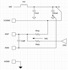
Hi - I'm looking at TPS548D22 - Is there any way of margining the output voltage of the device using an external D/A converter or PWM.

(please see Slaae23 - Voltage Margining and Scaling Circuit With Current Output Smart DAC (Rev. A) (ti.com) OR

slva845a -Design Voltage Margining Circuit for UCD90xxx Power Sequencer and System Manager (Rev. A) (ti.com) )

The default voltage is 0.75V and we would like to electronically margin the output so that it is settable between 0.675V to 0.825V i.e, 0.75V +/-10%.

Thanks

regards, Ranjeet

  •  

    Is there any way of margining the output voltage of the device using an external D/A converter or PWM.

    Yes.

    The Remote Sense Positive (RSP) pin is high high impedance, so you can place a resistor between the output voltage and the RSP pin to adjust the output voltage.  Just make sure VOSNS is still connected to the output voltage and not to the RSP pin.

    If you use the VSEL resistor to select 0.75V output and no resistor from RSP to RSN, the nominal output voltage will be 0.75V, even if you have a 1k to 10k resistor between VOUT and RSP.

    You can then adjust VOUT by driving a current into the RSP pin, to lower VOUT, or sinking a current from the RSP pin, to raise VOUT.

    For example, if you have a 10kΩ resistor from VOUT to RSP, each 1μA of current into the RSP net will lower VOUT 10mV  (1μA x 10kΩ = 0.010V).  If you drive 7.5μA into RSP, the output voltage will lower 75mV and margin VOUT down 10%.  Similarly, if you sink 7.5μA from the RSP net, the output voltage will raise 75mV and margin up 10%

  • We need to use the Remote sense as well. So is the solution to insert a 10K resistor between RSP and VOUT (VOSNS is connected to VOUT) and inject current into RSP from a D/A converter to margin? Will this work? Also - is there a formula that can be used to select the resistor value that is inserted in- between RSP and VOUT to set the output voltage?

    Thanks 

  • We need to use the Remote sense as well.

    Understood.

    So is the solution to insert a 10K resistor between RSP and VOUT (VOSNS is connected to VOUT) and inject current into RSP from a D/A converter to margin?

    Yes.  A 10kΩ resistor between Vout at the Remote Sense point and the RSP pin.  VOSNS needs to remain connected to Vout at the remote sense point.

    Will this work?

    Yes

    Also - is there a formula that can be used to select the resistor value that is inserted in- between RSP and VOUT to set the output voltage?

    The formula would depend on the DAC voltage or currents available.

    Vout = Vrsp + Rrsp x (Iadj)

    Where:

    Vrsp is the the RSP regulation voltage set by the VSEL pin

    Rrsp is the resistor value between Vout and RSP

    Iadj is the current drawn from  RSP into the DAC or adjustment source.

    If the adjustment is made with a DAC voltage and series resistor (Radj): Iadj is (Vrsp - Vadc) / Radj

    For example,  with a DAC voltage of 0-1V, VSEL selecting 0.75V and Rrsp = 10kΩ and a target adjustment range of +/- 75mV (10%)

    Maximum Sink Voltage is Vrsp - Vdac(min) = 0.75V

    Maximum Source Voltage is Vdac(max) - Vrsp = 0.25V

    Maximum Output Adjustment = Vout(max) - Vout(nom) = 0.075V

    Radj_max = Rrsp x Vadj(source_max) / (Vout(max) - Vout(nom)) = 10kΩ x 0.25V / 0.075V = 33.3kΩ

    When Vdac = 1V, Iadj will be (0.75V-1V) / 33.3kΩ = -7.50μA and the output voltage will be: 0.75V + 10kΩ x (-7.5μA) = 0.75V - 0.075V = 0.675V

    When Vdac = 0.5V, Iadj will be (0.75V - 0.5V) / 33.3kΩ = +7.5μA and the output voltage will be: 0.75V + 10kΩ x (7.5μA) = 0.75V + 0.075V = 0.825V

    Within the limits of the output current capabilities of the DAC, the resistors can be scaled together, but I would not recommend Rrsp > 10kΩ.

  •  

    Hopefully this will help clear up any confusion with the descriptions:

    Note:  I've added Cdiff, which is a differential filter between RSP and RSN.  It should be sized to form a time-constant less than 80ns (2MHz) with Rrsp to avoid reducing the phase of the feedback within the bandwidth of the control loop.

    It can also be useful to add a feed-forward capacitor from VOUT close to the inductor to RSP which can be populated to compensate for transmission delays between the local output at the inductor and Cout, and the remote sense voltage at the load.

  • The schematic and calculations discussed are when VSEL = 0.75V and RSP does not use any feedback resistors. 

    How does it work when feedback resistors are used ? E.g. VSEL = 0.6V , R1 = 2.55K, R2 = 10K  to achieve Vout = 0.75V 

    What is the formula to calculate Radj when feedback resistors are used?

  •  

    The equations don't change, just a couple of the factors going into the equations change.

    I assume by VSEL = 0.6V you mean that VSEL is configured to select Vrsp = 0.6V (100kΩ to BP and 4.64kΩ to AGND (for latch-off fault response) or 3.16kΩ for hiccup) 

    In that case, the Vrsp in the above equations would be 0.6V and Rrsp would be 2.55kΩ

    The current into RSP needed to lower VOUT from 0.75V to 0.675V would still be ΔVout / Rrsp = 0.075V / 2.55kΩ = 29.4μA

    The same current would need to be sunk from RSP to raise Vout from 0.75V to 0.075V

    The Adjust resistor needed to source 29.4μA of current from a 1V DAC with Vrsp = 0.6V would be (1V - 0.6V) / 29.4μA = 13.6kΩ 

    which is Rrsp x ( Vdac - Vrsp ) / ΔVout = 0.4V / 0.075V x 2.55kΩ = 13.6kΩ