This thread has been locked.

If you have a related question, please click the "Ask a related question" button in the top right corner. The newly created question will be automatically linked to this question.

LM5121: Disconnection Switch Issue

Part Number: LM5121

Dear team, 

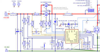
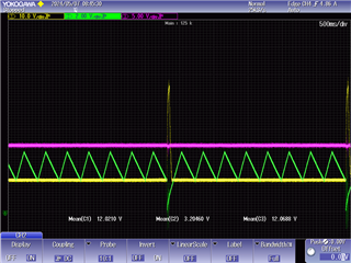
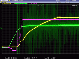
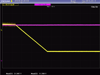
We have designed a boost inverter using "LM5121MHE". In case of having short circuit at the output I expect the NMOS T1 (As you see in the following photo) to open and shorten the input voltgae. But it seems that when there is a shortcircuit at the output, it just doesn't boost the voltage and I see the input voltage at the output. There is sth with this functionality (DG) that I don't understand. Can you take a look at the SCH and let me know if sth is wrong there?

Input: voltage 12V

          Current 7A

Output: voltage 48V

          Current 1.4A

Thanks in advanced

Farzaneh

  • Hello Farzaneh,

    Thanks for reaching out to us via e2e.

    I guess you mean to say that in case of a short on the output, T1 should disconnect the input voltage.
    But in the lab you (still) see the input voltage at the output.

    In case of an overcurrent, the LM5121 will NOT PERMANENTLY turn off the breaker transistor.
    Instead, it will enter a hiccup mode where it keeps trying if it can re-start regular operation.

    See datasheet, section 7.4.1 Hiccup Mode Short Circuit and Overload Protection:

    > If cycle-by-cycle current limit or inrush current limit is reached during any cycle,
    > a 30-μA RES current is sourced into the RES capacitor for the remainder of the clock cycle.
    > If the RES capacitor voltage exceeds the 1.2-V restart threshold, a hiccup mode protection sequence is initiated.

    > In the hiccup mode, the DG pin is discharged to GND if the inrush current limit is reached,
    > the SS capacitor is discharged to GND, both LO and HO outputs are disabled, ...

    So far, this is what you would expect. T1 is open and the device stops switching.

    > ... and the voltage on the RES capacitor is ramped up and down between 2-V and 4-V eight times.
    > After the eighth RES pin cycle, the DG pin is released and charged by the DG charge pump.

    So, after eight cycles where the voltage on the RES capacitor goes up and down between 2V and 4V (see figure 27/28),
    T1 gets enabled again, and you will see the input voltage on the output.

    Then the device will try to start boosting again and if it fails because of an overcurrent, the whole procedure will re-start again and again.

    If you do not like this behavior and you want T1 to remain open in that case, the datasheet describes how this can be done by using an additional Zener diode:

    > If a 2~3-V Zener diode is connected in parallel with the RES capacitor,
    > the regulator enters into the hiccup mode and never restarts until UVLO shutdown is cycled.

    Best regards
    Harry

  • Dear Harry,


    I have put the zener as it was indicated in datasheet and also your previous message. In case of having over current still I have 12V at the output. Then I removed the zener and the capasitor so the res pin connected directly to GND. It should cut the voltage reaching to 1.4A at the output. But what I can see is that while we increasing the current it reduces the voltage and never opens the circuit. 

    Regards

    Farzaneh

  • Hello Farzaneh,

    What does the voltage signal on the RES capacitor look like over time?
    Are you sure that the overcurrent is high enough to trip the hiccup mechanism?

    Thanks and regards
    Harry

  • Harry,

    I tested it for different current limits. At the output I have 48V as it is a boost converter. When I apply any of current limits I can see 12V at the output while I expect to see 0V. 

    Right now I have the circuit whithout zener and res capacitor.

    Farzaneh

  • Hello Farzaneh,

    So, the output voltage is basically the input voltage.
    But with a simple number we cannot really make progress here.
    We will need to look at Oscilloscope screenshots instead.

    One important test::
    Disconnect R5 or short R14 to keep the booster disabled.
    What do you see on the output when you supply power to the input?

    Do you already get 12V on the output, even if the contoller is disabled?
    If so, something is wrong with the breaker FETs (T1/T2).

    Best regards
    Harry

  • Dear Harry, 

    The first Photo is the circuit without zener, as you explained me before and by the datasheet I undertood that it should enter to hiccup mode if I put a zener in parallel with the Res capacitor. I don't have the zener and still it's in hiccup mode:

    Pink probe: input voltage 12V

    Yellow probe: output voltage 48V

    green probe:Res capacitor 

    We removed the RES Capacitor  to connect the RES pin directly to GND and this photo shows the result:

    In this photo it seems that the chip regulates the voltage. As we increase the output current it decreases the output voltage and the power consumption remains constant. 

    by the way I tested T1 and T2 as you have mentioned, they are OK.

    Looking forward to hearing from you

    Farzaneh

  • Hello Farzaneh,

    Thanks for the Oscilloscope screenshots.
    The first image shows that the fundamental hiccup procedure works.
    After eight triangles of the RES voltage, the controller is starting over, resets the RES voltage and tries boosting.
    But due to the overcurrent, the voltage on the RES pin exceeds the threshold and another eight triangles will start.

    The one thing that does not work is that the breaker transistors do not turn off.

    PLEASE DO NOT CONNECT THE RES PIN TO GND.
    This will probably damage the internal current source.

    Here again the test that I already asked for:
    Disconnect R5 or short R14 to keep the booster disabled while you power up the board.
    What do you see on the output when you supply power to the input?

    Do you already get 12V on the output, even if the controller is disabled?

    Then, enable the booster (with no load or light load) by connecting R5 or removing the short of R14.
    Your output voltage should then go up to 48V.

    When you then apply the short on the output, do you get the same hiccup cycles as in your first image?

    Please take oscilloscope screenshots which also show the voltage on the DG pin in addition to the RES cap voltage and the output voltage.

    Thanks and regards
    Harry

  • Here you can see the screenshot. I tested the T1 and T2 , they work. I wanted also to ask a question, we connect mode pin to GND. could it be the problem?

    The green probe is DG.

    Thanks


  • Hello Farzaneh,

    First, I want to apologize.
    I had overlooked that the LM5121 does include some logic which allows you to connect the RES pin to GND to disable the hiccup feature.
    So, there is no risk for a damage there.

    You wrote:
    > I tested the T1 and T2.  they work.
    How did you test that? Can you somehow turn them on and off?

    Anyway, what I would like to see in an oscilloscope screenshot is the behavior of the breaker FET control (the signal at the very bottom of Figure 27.

    I must admit that only looking at DG versus GND may not be good enough.
    Can you please also probe the Ds voltage?
    If you have a differential probe it would be great because you could directly measure the difference.
    If not, please measure DG and DS and show both of these signals on top of each other.
    If possible, use the math function of the oscilloscope to calculate the difference.
    (If you do that, please be aware that there may be glitches due to different timing offsets of the two oscilloscope inputs).

    I would like to see when the VDG - VDG goes low to turn off that FET.

    And, again, I would also like to see what happens at the initial power-up.
    When does that FET get turned on?
    You may need to set some trigger on your oscilloscope (e.g, when the UVLO voltage exceeds a limit) to catch that point.

    Thanks and regards
    Harry

  • Morning Harry,

    I cheched the T1 and T2 as you have explained me. I removed R5 and I didn't observe any voltage at the output. So according to your explanations if it is so, it means that they are OK. Placing back R5 I observed 48V at the out put. By the way I changed the PCB and I took a new one to descart any damaged cuased by testing. 

    Following you can see the screenshots of what you asked for:

    starting up:

    Yellow probe :Output

    Green probe : UVLO

    Pink probe : DG-DS (differential probe)

    Connecting load:

    Yellow probe :Output

    Pink probe : DG-DS (differential probe)

    I appreciate your time and attention

    Farzaneh

  • Hi Farzaneh,

    Due to bank holiday, please expect a reply by Friday.

    Best Regards,

    Feng

  • Hello Farzaneh,

    Thanks for the additional screenshots.
    The inrush current limiter also works fine and the breaker FETs are controlled correctly at that time.

    So, I assume the following:
    The overcurrent that you apply is not high enough that it would (permanently) exceed the circuit breaker threshold:
    VCS-TH3 Circuit breaker enable threshold CSP to CSN, Rising: 170 mV (max)

    If the voltage drop on the sense resistor does not exceed 170mV, the breaker will stay ON.

    The hiccup mechanism is independent and even if the breaker is not tuning off, it will show these 8 cycles, as seen in your previous screenshots.

    Best regards
    Harry

  • Morning, Harry,

    I wanted to express my gratitude once again for your invaluable support and thorough explanations. Thanks to your guidance, we've finally managed to decipher what was causing the issue. It seems there was a misinterpretation of the datasheet on our end.

    Upon closer inspection of the attached photos extracted from the datasheet:


    We initially concluded that both overcurrent and short circuit instances would trigger T1 and T2 to open, thereby cutting off the output. However, our observations have revealed a discrepancy. While a short circuit does indeed result in an output voltage of "0," in the case of overcurrent, we're perplexed to find that the input voltage persists at the output.

    It appears you were correct in your assessment that we weren't subjecting the system to sufficient current to observe the expected output voltage drop to "0."

    Thank you once more for your patience and guidance in navigating this issue.

    Farzaneh


  • Hello Farzaneh,

    Thank you for the feedback.

    I understand that especially the second image might suggest that all the shown signals would always happen in this combination and that the word "overload" is not clearly defined.
    Only the Electrical Characteristics table will tell you that the circuit breaker uses a different / higher threshold.

    I am glad that I could help to clarify that.

    May I please ask you to close the thread?

    Thanks and regards
    Harry