


I'm using the design provided by Webench
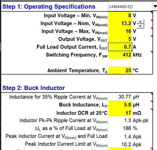
The forum seems to be filtering the Webench design link below. The design parameters are Vin: 8V to 16V with 13.2V nominal. Vout = 5V fixed, Iout: 0 to 0.7A, 0.1A nominal
link: Webench design
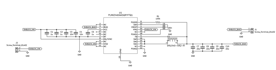
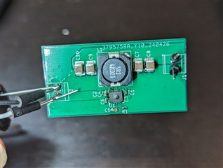
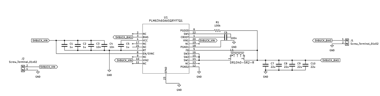
link: Schematic (IC is actually LM64460 not LM63460 indicated in schematic)
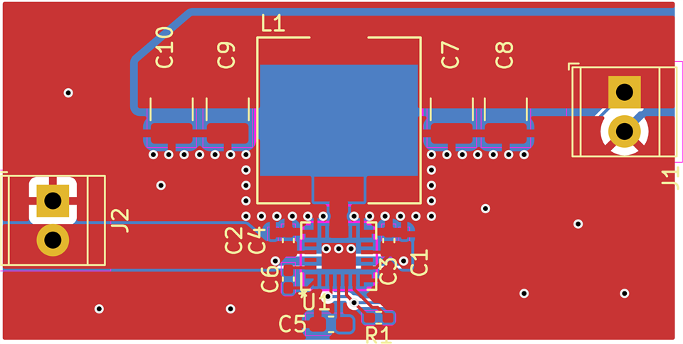
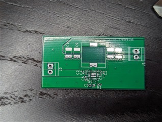
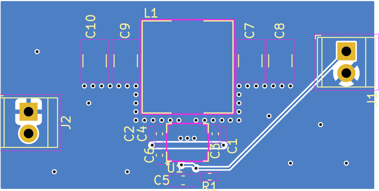
link: PCB Top
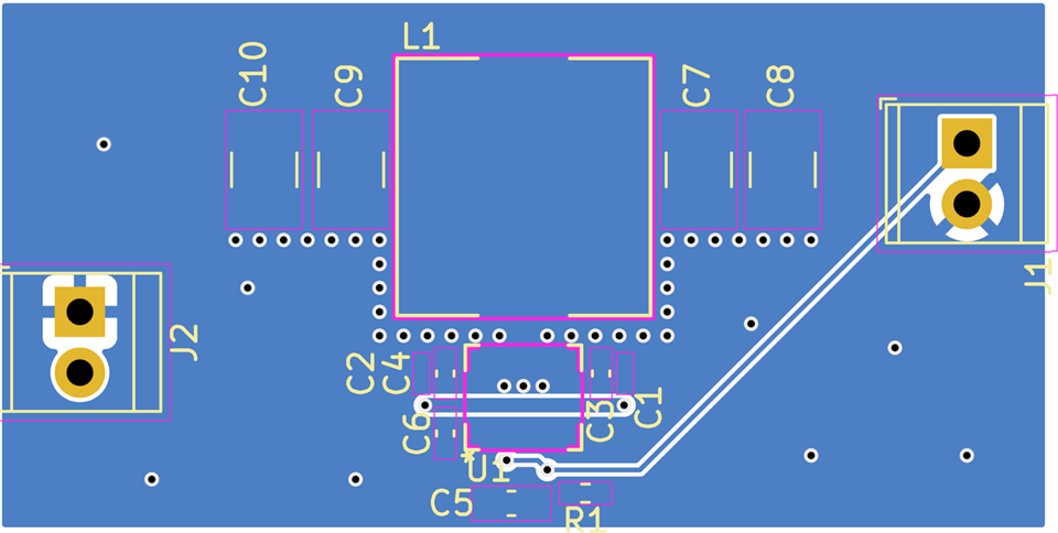
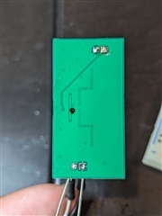
link: PCB Bottom
I am testing with no load, and the IC keeps overheating. After failure I am finding SW1/2/3 conductor of the IC shorted to GND, so I suspect the internal mosfet is failing.
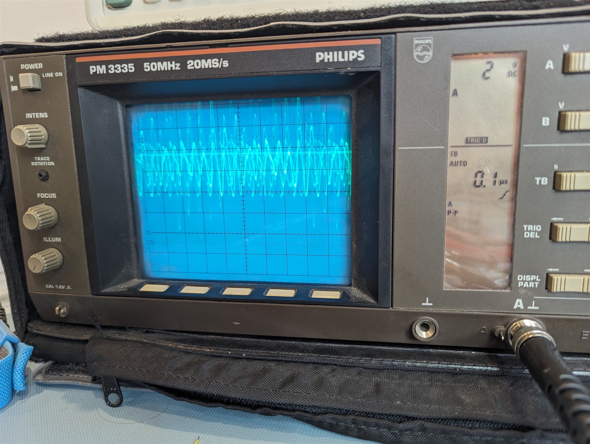
For the first prototype I tested by slowly ramping up Vin and watching for high input current. A high sustained input current (1A) was observed starting at around 4V. As I increased Vin it dropped to a few mA however Vout was only 1.2V. Finally the input current dropped to 0A and Vout was 0V, at this time I discovered SW1/2/3 shorted to GND so the chip is destroyed.
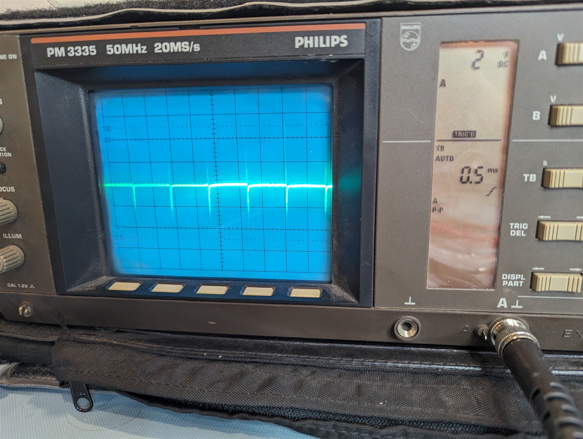
For the second prototype I set a 100mA current limit on my bench supply, this allowed Vin only to reach 4V before reaching the current limit. I captured some waveforms and can share if valuable. I later removed the current limit and tried to apply 12V Vin in a step-wise fashion, the input current was stable at ~15mA for several seconds before shooting to 3.2A (the max of my bench supply) sustained and smoking of the IC.
Is there anything wrong with the schematic or layout that would likely cause this behavior? Is this design able to operate with no load or is there a minimum load requirement? Is failure or damage expected from current limiting the input supply?


