This thread has been locked.

If you have a related question, please click the "Ask a related question" button in the top right corner. The newly created question will be automatically linked to this question.

LM5156: Power Output Issues At Full Load

Part Number: LM5156

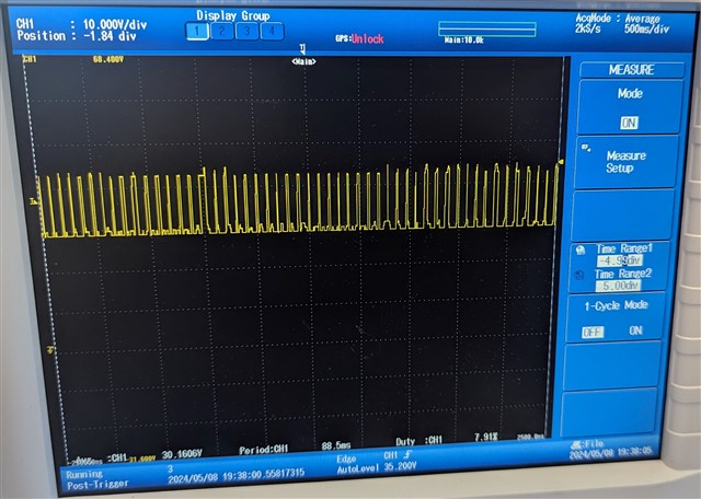
I have been tasked with testing someone else's design using the LM5156HPWPR chip and am having issues with delivering power at load. Smaller loads work as intended, but when I swap to the intended load it fails to deliver the output voltage and you can clearly hear clicking/switching coming from the board.

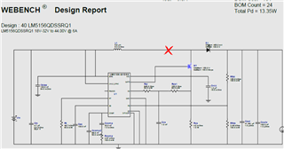
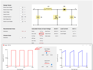
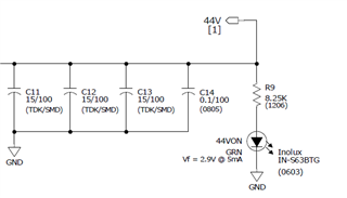
The designer seemed to very closely follow the design suggested by the WEBENCH tool, with the only significant differences I see being the addition of LED indicators.

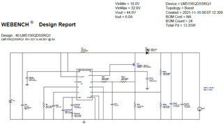
I am fairly confident our supply is not the issue and while I have not gone over every trace I would broadly trust the designer's layout ability. I've familiarized myself with the chip and the datasheet and have not yet noticed any obvious errors. Any Input on the steps I could take isolating where the issue might be would be greatly appreciated!

  • Hi Marsh,

    Thanks for using the e2e forum.

    There can be several reasons for the device not being able to support the full load at the output.
    As the information on the behavior we have right now is rather limited, I would kindly ask you to go through the following checklist to find the root cause:

    - Is the power supply strong enough and there is no drop of VIN? (already been checked)
    Are power stage components rated for the required power? (Inductor saturation current, diode DC current, MOSFET)
    At worst case conditions (min VIN, max load) I would expect peak inductor current up to 17A, so please make sure the inductor can support this
    - How does the VOUT and SW signal look during operation?
    Checking these two signals will show if the regulation system becomes unstable or oscillates at higher loads, which would indicate non-ideal compensation
    - Is the device reaching over-current-protection (OCP)?
    A measurement of the CS pin voltage will show if the device runs with duty cycle limitation as the cycle-by-cycle current limit is triggered

    Please let me know if you have additional questions.
    Thanks and best regards,
    Niklas

  • Thanks for the quick reply! For the quick / easy checks...

    1. i believe the power supply is good for our intended load but as a sanity check, it is rated for 0-35V and 0-10A. My testing so far has been with loads of 75Ω / 225W and 10Ω / 225 power resistors. The 75Ω load was the 'safe' system check and the 10Ω is the approximation for our intended load.

    2. Apologies, I should have mentioned that I checked over most of the components and they seemed to match or exceed the recommendations.

    Inductor – 28A, 21A Saturation – Vishay IHLP6767GZER5R6M11

    MOSFET – 150V / 130A – IXYS IXTA130N15X4

    Diode – 20A – ST Micro STPS20M100SG

    As for 3/4, the board as is does not have convenient test points so this will take a bit of solder work. I'll try to check these out and get back to you with some info / scope signals as soon as I can. 


  • Hi Marsh,

    Thanks for the update.
    I agree that the components for inductor, FET and diode should be able to support this application.

    I am looking forward to the scope measurements.
    Thanks and best regards,
    Niklas

  • Just to clarify, by 'SW signal' do you mean the output at the RT pin? I am also assuming VOUT is what the datasheet refers to as VLOAD rather than the bias or VCC. 

  • Hi Marsh,

    The switch node (SW) refers to the point between inductor, output diode and FET.
    I marked it on the schematic:

    Vout is the same as Vload, this is correct.

    Best regards,
    Niklas

  • Some measurements from just now. Everything at 75Ω was quite stable as far as I could tell. Vsense and VSW signals both seemed pretty flat on the scope, a little noise but no periodic behavior that stood out to me. 

    75Ω load -
    Vsense = 2.8mV
    VSW = 27.928 V
    VOUT = 43.10 V

    10Ω load -
    Vsense = 5.8 mV
    VSW = 27.488 V
    VOUT = ~30 V - see image for scope reading


    I captured average voltage, period, and duty cycle. Let me know if I should be focusing on something else!

  • Hi Marsh,

    Due to bank holiday, please expect a reply by Friday.

    Best Regards,

    Feng

  • Hi Marsh,

    Thanks for performing the measurement.
    It looks like the device is running with a duty cycle limitation. This would also explain why the output voltage is dropping to 30V

    To calculate the expected duty cycle of a boost design, you can use the Power Stage Designer tool, which looks like this:

    https://www.ti.com/tool/POWERSTAGE-DESIGNER

    The typical reason for duty cycle limitation is the triggering of over current protection (OCP).
    The OCP level is set via the current sense resistor. Right now you are using a 4mOhm resistor for this, correct?

    Could you please double check the design with our quickstart calculator tool to see if a lower sense resistor is recommended?
    The tool can be found here:
    https://www.ti.com/tool/download/SNVC224

    Best regards,
    Niklas

  • Thanks for the links. looks like the expected duty cycle should be in the ballpark of 60%. 

    As for the quick start tool, perhaps I am not using it correctly but I am not seeing any real change from the 4mΩ sense resistor we are using. As a sanity check, i compared our design with that which was provided by the the WEBENCH tool given an input voltage range of 18-32V, a nominal voltage of 28V, an output voltage of 44V, and a current of 6A. Everything looks good, with the sole difference I see being the indicator LED shown below.

    I would be happy to try swapping in a different sense resistor but am not sure what the value should be or what factors would indicate that change was the issue.

  • Hi Marsh,

    Thanks for the update.
    I went through the calculations myself and 4mOhm should indeed be a good sense resistor value.
    This sets the OCP limit to 25A, which leaves a healthy margin to the expected peak inductor current of ~ 18.5A.
    The indicator LED from the reference should not have any effect either.
    It is also possible that the OCP is falsely trigger through noise on the CS pin, but the webench schematic implements an RC filter for this exact reason, so I would not assume this is an issue here.

    A notable difference I saw between webench schematic and the quickstart tool is the output capacitance.
    Webench seems to use 40uF, but I would recommend at least 100uF to higher stability and lower output voltage ripple.
    Ceramic capacitors also have higher DC bias derating, so the actual inductance at 44V output voltage may be lower.

    What is the output capacitance used in your design?
    And can you point out any other differences between your design and the webench schematic?

    Thanks and best regards,
    Niklas

  • Thanks for the quick responses and for looking into this!

    I didn't recall the CS pin being particularly noisy but I can have another look in case that is an issue. 

    As for the output stage, it looks like we already added a little extra capacitance but certainly not on the order you are talking. We can certainly look into improving the output capacitance.

    The only other difference I see (beyond the already mentioned LED indicators) is a TVS diode at the input. Though now that I am checking things again I see the input capacitance is a little lower than the 4.7uF recommended.


    Output:

    Input:

    For your reference:

    C1 / C2 / C3 / C4 = 1uF / 100V / ceramic - C3216X7R2A105M160AA

    C11 / C12 / C13 = 15uF / 100V / ceramic - CKG57KX7S2A156M335JH

    C14 = .1uF / 100V / ceramic - GMC21X7R104K100NT

  • Hi Marsh,

    Thanks for the update.
    Input capacitance is of lower importance than output capacitance for a boost topology. As long as there are no drops on the input voltage signal, there should be no problem.
    Regarding output capacitance, please account for derating as mentioned before.
    The compensation network placed in the webench schematic should be stable for Cout of 100uF, but may not be ideal for 40uF or less effective capacitance.
    Please use the quickstart tool to visualize the bode plot stability for this. ( https://www.ti.com/tool/download/SNVC224 )
    We recommend a phase margin of 60 degree or more for a stable system.

    Best regards,
    Niklas

  • Thanks for your input. Our input signal has always looked fine as far as I can see. I will be sure to keep an eye on it moving forward, just to be safe. 

    I can't find large enough capacitors in stock anywhere that would be drop-in replacements for our current footprint. I was initially leaning toward trying to swap in an electrolytic capacitor (unless you had some concern) but I might just try to make a different size ceramic work.

    I doubt we have the appropriately rated parts on hand, but I'll check things out when I can and then report back. 

  • Hi Marsh,

    Thanks for checking.
    As we are currently in the debugging process, it might not be required to find caps with the exact same footprint.
    If it is meant for just one startup test with different output capacitance, you can take an electrolytic cap and just connect it somewhere close to the output stage or even stack caps on top of each other or use short wires. If the results look promising, we can look for suitable part numbers or required layout adjustments afterwards.

    Best regards,
    Niklas

  • sorry for the delay! it took a while to get parts in and then have time for more testing.

    i swapped the 3 ceramic 15uF caps in parallel with 3 aluminum 33uF caps and the circuit performed as expected! both output voltage and current looked great with the values we would expect.

    thanks for your help! we will move for a re-spin of the board now. we will keep our layout as close to the same as we can while making the capacitor adjustments and adding a couple more test points. 

    any further input on recommended capacitors or any other tweaks before we re-spin would be quite welcome. thanks for your help in stepping through all of this!

  • Hi Marsh,

    Niklas is out of the office but can comment till end of the week.

    Best regards,

     Stefan

  • Hi Marsh,

    I am glad to hear the behavior improved with larger capacitance.

    There are no other required chances I see right now. For the next revision, a general recommendation is to place some additional footprints for output caps, gate resistor and RC snubber circuit at the forwarding diode.
    This way additional fine-tuning can be performed much easier if necessary.

    Best regards,
    Niklas