


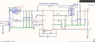
I am having a Boost converter design
the design requirements are
| Vin Min | 6.9 |
| Vin Max | 8.4 |
| Vout | 30 |
| vdiode | 0.5 |
| Iout | 1 |
| FSW In mhz | 0.37 |
Based on this the calculated inductor values are
| L1@Vmin | 8.3 |
| L2@Vmin (CCM operation) | 3.3 |
| L1@Vmax | 11.4 |
| L2@Vmax (CCM operation) | 4.6 |
I have selected 4.7 uH due to space constrain IHLP2525CZER4R7M11
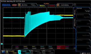
I was trying to bring up the design the output of the boost converter is oscillating when the load switch is turned on to charge the capacitor
when I load the output the converter output rail BOOST Converter out is oscillating and the output is charging quickly due to current limiting not set properly
so I recalculated the values
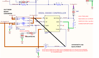
Because of the input limitation the boost converter output current to be Limit need to be limited to 0.5A based on the datasheet the calculated values of Rsns RS1 and RS2 are
| ILIM | 0.5 | |
| rsns | 0.016033413 | 0.015 |
| power Dissipation In RSNS | 0.2333786 | |
| rs1 | 110 | limited to 500 |
| rs2 | 12088.65205 | 12103.56421 |
are the above values correct ?
Is there a option in we bench or any spreadsheet tool available to design boost converter with LM5022MM with custom values And check the response of step load
We bench is not allowing to change values as we wish .. it is optimizing values based on the optimization strategy used

