This thread has been locked.
If you have a related question, please click the "Ask a related question" button in the top right corner. The newly created question will be automatically linked to this question.
Dear support team,
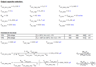
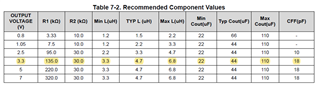
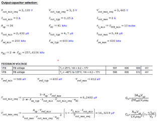
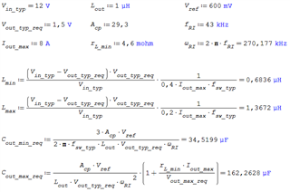
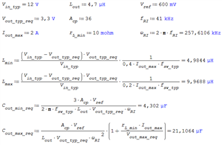
in the datasheet of the TPS562203, a max. output capacitance of 110uF is recommended:
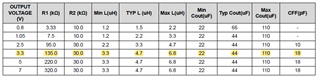
I cannot find any restrictions / calculations in the datasheet about the output capacitor.
In our application we are using a lot of decouling capacitors at the separate ICs which gets supplied from this power supply - in sum we have >100uF.
Do you see any problems, when driving a higher capacitance at the output? How can I determine the max. output capacitor?
Thank you for your support and kind regards,
Markus
Hi Markus,
I am looking into this, I will respond to you by tomorrow. Thanks!
BRs
Lucia
Hi Markus,
It's for the stability criteria consideration. You can refer more Stability Analysis and Design of D-CAP2 and D-CAP3 Converter – Part 1.
BRs
Lucia
Hi Lucia,
for calculating the output capacitor range, I would need the A_cp / Omega_RI value of the TPS562203. I could not find any of these parameters in the datasheet. Can you share these values with me?
Kind regards,
Markus
Hi Markus,
Pls kindly let me check and get back to you soon. Thanks!
BRs
Lucia
Hi Markus,
The internal ripple injection high-frequency zero is about 41kHz. (You can find it in datasheet). Acp is 36.
If you think it's resolved, can you please close the thread by clicking on resolved. Clicking the Resolved Button also helps us to maintain this forum. Thanks! Stay safe and have a great day!
BRs
Lucia
Dear Lucia,
I have now tried to calc. min/max value of the output capacitor. Could you please review my calculations below:
It seems, that my results are different to the TIs recommendation:
What do you think about it?
Kind regards,
Markus
Hi Markus,
I will review your calculation and it may take some time. Will give you feedback soon.
Thanks!
BRs
Lucia
Hi Markus,
It discussed about large duty operation. But what will be the input voltage range of your application?
Thanks!
BRs
Lucia
The nominal input voltage range is 12V +/- 10%. But in case of supply interruption tests the 12V are buffered with >5mF and therefore the input voltage slowly falls and this buck shall operate as long as possible. In this case the duty cycles will be higher than in normal operation.
Additionally the frequency will be reduced during light load operation.
Hi Markus,
Pls kindly let me check and I will get back to you before end of this week.
BRs
Lucia
Hi Markus,
In your equation, Fsw can be set as 600k. And the internal ripple injection high-frequency zero is about 41kHz, so wRI=2*pi*41k. Pls kindly correct it.
Thanks!
BRs
Lucia
Dear Lucia,
I have updated my calc. accordingly:
Unfortunatelly, again the result does not match with the TI recommendation.
Hi Markus,
Do you consider that the ceramic capacitor has DC bias de-rating? As you can see from datasheet, the typical Cout is norminal value. I think what you calculated here is effective value.
Thanks!
BRs
Lucia
Hi Lucia,
currently I havent chosen any capacitor at all. I only want to calc. the min. and max. output capacitance, which is needed / allowed for the power supply. For this calc. I used your recommended application note (SLVAF11).
My last calc. results into a output capacitance of 8,2 ... 16,3 uF and the TIs recommendation is 22 ... 110 uF. Even with DC-bias this makes no sense.
-------------------------------------------------------------------------------------------------------------------------------------------------------------
Additionally I tried to check, my calc. against the example in the application note:
Now I realized, that for this example, only typical values are taken - in both cases the Cout calc. is 35 ... 163uF.
-------------------------------------------------------------------------------------------------------------------------------------------------------------
After this i redo with my typical values:
But again, the TI recommendation is different.
Kind regards,
Markus
Hi Markus,
Pls kindly let me check and get back to you before end of today. Thanks!
BRs
Lucia
Hi Markus,
1. The typical Cout mentioned in datasheet is norminal value, not the effective value after derating.
2. When Vout is higher, Cff will be benefit to the loop stability. You can also find more details about Stability Analysis and Design of D-CAP2 and D-CAP3 Converter – Part 2
Thanks!
3. In general, when we design our devices, we simulate a couple of LC combinations and also validate a couple of those combinations in our labs and those combinations are then recommended in the datasheet. We cannot generalize the maximum allowed output capacitor based on that the system might differ in the actual design, for example, different inductance, different DC bias voltage characteristics of ceramic capacitors, tolerance, aging and temperature effects.
Thanks!
BRs
Lucia