This thread has been locked.

If you have a related question, please click the "Ask a related question" button in the top right corner. The newly created question will be automatically linked to this question.

TPS61253A: Stuck in Pass Through Mode during charging

Part Number: TPS61253A
Other Parts Discussed in Thread: BQ25896

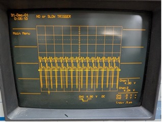
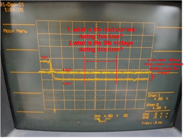
We are using the TPS61253A in forced PWM mode, to supply 5V to some heaters from single li-ion cell.  Generally it has been working well. On some boards if the chip is operating while the system is charging, at 5V, it seems to get stuck in pass through mode.  Even after the charging has been disconnect the output will continue to fall with the system voltage/input voltage to 4.2V or lower.  It appears to be stuck in pass through mode.  Reseting the TPS61253A will return it to controlling the voltage, but this is somewhat undesirable from a performance perspective.  Any advice on why this might be happening and how to prevent it would be appreciated.  Thank you

Jeff

  • Hi Jeffrey,

    Thanks for using E2E.

    It sounds like a strange behavior. Can this behavior be reproduced stably? Or still occasionally appearing?

    If possible, could you please share schematic including charging?

    May I know the output current of TPS61253A, especially when when charging starts and stops?

    Could you please share some waveforms like the VIN, VOUT, SW node voltage of TPS61253A?

    Regards,

    Nathan

  • Dear Nathan,

    Thank you for your reply.  I'll do my best to answer your question.  It is an occasional problem that I am not able to reproduce on command, though it is a regular problem.  I'd estimate that on average it will occur after running for 8hours on a charger.  Here's the schematic for the TPS61253A:


    And for our charger:

    The output current is variable. It feeds a pair of resistive heaters that maintain a temperature set point.  These cycle on and off.  The max current would be around .7A, min would be at or near zero.  Over all the heaters duty is very roughly 30%.

    I've done my best with the waveforms on our ancient oscilloscope.  As this is an occasional problem these are from a system that was in spec so might not reveal much.  I'll leave it running and charging and see if I can capture those waveforms.

    SW:

    Vin:

    Vout:

    Thank you again for your help and advice or guidance you can provide would be much appreciated, we're a bit stumped obviously.

    Best

    Jeff

  • Dear Nathan,

    As an update the board failed in the same maner with the TPS61253A shortly after I posted the above.  I captured waveforms in the faulty state:

    SW:

    Vin:

    Vout:

    Cheers:

    Jeff

  • Hello Jeff,

    I'd estimate that on average it will occur after running for 8hours on a charger

    Do you mean that for each board, it will occur after running about 8 hours? I want to make sure that if this behavior will vary depending on the chip or not, if it occurs on each board or not.

    And more, I can't get a clear information from the waveforms, for example, what is VOUT VIN voltage? From the waveforms, only a line but not zero scale so I don't know what is voltage now.

    And it would be helpful if you can capture the waveforms at the moment when the device starts to behave abnormally. Maybe not easy but would helpful if you can.

    Thanks.

    Regards,

    Nathan 

  • Dear Nathan,

    Thank you again for your help.  I'll do my best to address your questions, let me know if I miss anything.

    The 8 hours was just an average for brevity.  The longer answer is we've tested 6 boards, all have shown this behavior with the TPS61253A, on multiple occasional.  Sometimes the chip will maintain the appropriate 5V out for only 1 hour sometimes for over 12 hours.  Generally they fall out of spec after about 4-8 hours on a charger.  We've never seen any of the board's TPS61253A go out of spec if they are running solely off the battery. We charge the system at 5V, that input would come from a wall wart into the V_Charger rail in the above schematic.  Let me know if that's clear or if you think some additional details would be helpful.

    Sorry the waveforms weren't clearer, I had used the AC coupling to zoom in on the changes.  I can tell you consistently when the system is in spec Vin is 4.2V Vout is 5V.  When out of spec Vin is still around 4.2V and the Vout is following that closely, is just under 4.2V.   I'm not sure how to capture that transition, I suspect it's occurring on the order of a couple ms once per 4-8 hours, do you have any suggestions?  I'm open to getting new equipment within reason.

    Let me know if that sparks any ideas or if you have any additional questions.

    Best,

    Jeff

  • Hi Jeff,

    Thanks for the explanation.

    Sounds like that each part would have this problem.

    For the waveforms, I think you can set the trigger condition as VOUT falling, trigger voltage at about ~4.3V, and the trigger type at Normal or Single. Then when the VOUT of TPS61253A drops from 5V to 4.2V,  the waveforms should be stopped at the moment.

    Please also attach 5V_EN signal waveform, and if possible, output current waveforms or inductor current waveforms of TPS61253A would also be helpful to analyze.

     Are you trying with different MODE status? I found you connected MODE with 5V_EN, how about connecting it with GND or leave it floating? I am not sure if it is related to problem, just want to find something.

    Regards,

    Nathan

  • Dear Nathan,

    Thank you for that suggestion.  I will work on getting those waveforms, it might take me a little bit as these are on form factor boards so there isn't a lot of space to work with for probes connection ect.  Relatedly I'm not sure if I can at the moment change the MODE status. We've hardwired that to the 5V_EN line, so if I ground or float that line the TPS61253A will turn off, I believe.  Maybe a can modify an existing board to see about splitting those lines.

    In the meantime, do you have any theories as to what might be happening?    I'm not sure if I mentioned, but this is our third run of this design after a prototype design.  The prior runs didn't  have this issue.  We're in a little bit of a pickle, as while there might be some work around, we were hoping to start delivering these boards to customers this week.

    Thank you again appreciate your help,

    Jeff

  • Hi Jeff,

    Unfortunately I don't have a clear idea about the cause by now, but can give some thoughts.

    For pass-through mode, usually when the VOUT is lower than target VOUT, 5V for TPS61253A, it will exit pass-through mode and enter Boost mode.

    There are another two possible conditions that the device would stuck in similar pass-through mode.

    1. If the VOUT is soft shorted by something like a very large load current  (even higher than current limit), or shorted by a small resistance at VOUT node. It may be stuck in high-side FET on condition, looks like as same as pass-through mode. The device will not exit this condition until you remove the soft short.

    2. If the device enters in DC startup mode due to some reasons, like output short, overload, UVLO or maybe there are some noise at EN, the high side FET will also be turned on, also looks like pass-through mode.

    How about adding some RC noise filter at EN? Or place a small capacitor, like 10nF, 100nF at EN to ground? 

    I am not sure if there is something like unplugging and plugging when you start the charging at 5V, maybe there some noise caused by hot plugging.

    Do you have any pull-down/pull-up resistor at EN? It is not recommended to use >1M ohm as this would introduce noise to EN pin.

    Regards,

    Nathan

  • Dear Nathan,

    Thank you for those theories.  Does seem like some possibilities.  I have been working through the troubleshooting I can from them along with trying to capture some waveforms via your suggestion of using a trigger off the Vout, and have had some success. Thank you again for that suggestion.  Though as the error is sporadic I have only capture a couple errors:

    Here's the SW line channel 2, and the Vout on channel 1 with the trigger before the error/trigger:

    and after the error, which I think just shows the lower voltage.

    Here is Vin as compared to Vout when it falls:

    I don't have a lot of access to EN line to test.  I was able to switch it from no pull up to having a pull up, via the microcontroller, but that didn't seem to have much effect.

    Let me know if that sparks anything, in the meantime I'll keep investigating some of the other possibilities.

    Thank you again,

    Jeff

  • Hi Jeff,

    From fig.3, it looks like, there is a inrush at VIN, VIN rise to about ~5V. I guess this is the moment when charging 5V starts, there are some inrush current at VIN.

    And more, the voltage drop between VIN and VOUT in fig.3 is about ~400mV (need to double check), it is larger than what I think. In pass-through mode, the voltage drop is caused by the inductor resistance (DCR) and the high-side FET resistance.

    And more, may I know your inductor DCR?

    For example, if the DCR is 40mohm, high-side FET resistance is 60ohm, 400mV voltage drop means there is 4A load current. 

    Is it possible that the load current of TPS61253A becomes so large when the charging 5V starts? If that, it may stuck in pass-through due to the condition below.

    1. If the VOUT is soft shorted by something like a very large load current  (even higher than current limit), or shorted by a small resistance at VOUT node. It may be stuck in high-side FET on condition, looks like as same as pass-through mode. The device will not exit this condition until you remove the soft short.

    And more, could you please clarify the question in the figure below?

    Regards,

    Nathan

  • Dear Nathan,


    Thank you again for taking a look, and taking a look at the waveforms I was able to capture. I think the monochrome oscope I have makes it a little more difficult, but you essentially have the same interpretation I do, but with a couple corrections.  I’ve highlighted channel 1 and channel 2.  The values on the right box, refer to the reference cursor which is the dash dot line.  I had put it right at 4.2 V for channel 2 as I thought that was relevant but that made the offset different – the channel 1 vertical scale is 300mV above the channel2 scale.  So Vout (Ch1) and Vin (Ch2) are much closer. I make Vout and Vin to be close to the same value just under 4.2V:

    As to your questions on the graph.  I didn’t measure the SW voltage at the time, but from the previous figures which were capturing similar failures, I make the SW voltage to be a little bit under 4.2V as well.  I don’t have a measure of the load current independently, but Vout supplies a pair of resistors with an equivalent R of about 7Ohm, so unless there is a temporary short the load current should be about 700mA (max).  The current to the resistors are controlled by FETs that switch on and off to maintain temperatures.

    The other point to clarify is the spike evident in figure 3 doesn’t correspond to the charger being attached.  The charger has been attached for at least several minutes to an hour, this is the captures via the trigger during that running.

    The Inductor’s DCR is 26mOhm.  It’s PN: IHLP1212AEERR82M11 From Vishay Dale is that’s helpful.

    I think understand your theory about the Vout short, and the TPS61253A looking like it’s in pass through mode, but pinned.  I’ll see if I can find a short, but so far I haven’t seen other evidence. (The board isn’t heating up, I haven’t noticed large current draws.  Also this only happens when connected to a charger, so the short would have to be related to a charger being connected? )


    Do you have any suggestions on hunting for this possible soft short, or any other ideas? I’m trying to recapture that failure to double check, but so far it hasn’t happened today.


    Thank you again,
    Jeff

  • Hi Jeff,

    If VIN VOUT SW are all about ~4.2V, seems like the VOUT short or large load current is not the possible reason.

    I will make some test in our bench to see if it can be reappeared in our lab.

    By the way, do you know why VIN sometimes increase to as high as 5V suddenly? Do you mean that there is no action at this moment, but the VIN increase?

    Looks like this VIN increasing cause the problem. How about adding larger input capacitors of TPS61253A? 

    The charger has been attached for at least several minutes to an hour, this is the captures via the trigger during that running.

    Regards,

    Nathan

  • Hi Jeff,

    After discussion with design team, looks like it is because that the input voltage increases and decreases too fast for some internal comparator to operate normally.

    So maybe you need to find out why there is an abrupt change of input voltage and try to remove it. Or we recommend to add larger input capacitance so that the slew rate of input voltage could be slower.

    Regards,

    Nathan

  • Dear Nathan,

    Thanks for taking a look and discussing.  I'm not sure why that input voltage is increasing then decreasing - should be regulated by the charging the chip, the BQ25896. I know that's a little outside the scope of this discussion, but it is another TI part, is there any thing you know about it let through a voltage change like that? I do know that increase and decrease that is being discussed is definitely not from something we are doing intentionally, but I'll take a further look. 

    There is already the recommend bypass capacitor there 10uF, by larger are you thinking like 100uF?

    I will do some more investigating and can try a larger cap.  Though I'm traveling for the next 3 days, so it'll have to be at the end of the week.

    Thank you again for your help,
    Jeff

  • Hi Jeff,

    About the BQ25896, maybe there is a inrush current flow into V_SYS, or there is a abrupt change of the V_CHARGE (input of BQ25896), or there is some mode transition at this moment of the charger.

    Maybe the V_SYS abrupt change doesn't caused by the charger, it may be caused some other devices that connected to V_SYS.

    Even there may be a reverse current flow into the battery from V_SYS nodes so that the battery voltage increase and then V_SYS increase. Not sure the specific cause.

    About the input capacitor, it is hard to give a boundary here, 100uF is of course ok. You can add one and have a test to validate.

    And more, because this thread is too long to read, I will close it. If you have any more question, you can post a new thread, I will support you further.

    Regards,

    Nathan