This thread has been locked.

If you have a related question, please click the "Ask a related question" button in the top right corner. The newly created question will be automatically linked to this question.

UCC28950: equivalent circuit or functional block diagram looking into DELAB, DELCD pin

Part Number: UCC28950
Other Parts Discussed in Thread: TINA-TI

Hello,

I am requesting an equivalent circuit or functional block diagram looking into DELAB or DELCD pins.  I need to reduce the dead time at heavy loads to increase efficiency while increase the dead time at light loads to allow ZVS.  I am already using adjustable delay, which is helping, but doesn't allow me to accomplish the above to the extent needed.

My goal was to reduce the effective value of resistance connected to the DELCD pin (as seen by the UCC28950 controller) at heavy loads...I was hoping that have a functional diagram looking into the DELCD pin would help me determine a way to do that.

Any suggestions would be appreciated.

Thank you,

Nitish Agrawal

  • Nitish,

    If I understand it correctly, you'd like to sink/source additional current from the DELCD pin at different load conditions to have larger dead time range, right? Please confirm.

    You could adjust the Ka value by increasing the Ra to Rahi ratio. The max value of Ka is 1 and it will give you more weight on CS pin voltage, which is proportional to the load.

    I am not sure about the typical CS voltage in your application. You can also consider to increase the CS voltage without triggering the protection in normal operation. In theory, the biggest ratio you can have between light load and full load for deadtime is 11:1. In real applications, the ratio is in single digit.

    Please keep in mind that CS voltage also affects other settings like adaptive delay so please tune it carefully.

    Best,

    Ning

  • Hi Ning,

    Thank you for your response.  Your understanding is correct that I would like to sink or source additional current from the DELCD pin at different load conditions to have larger dead time range.  More specifically, I would like to decrease the resistance connected to the DELCD pin at full load as seen by the UCC28950 controller.

    I have already tried adjusting the KA value.  I have already increased the CS voltage at full load....which is ~1.8V peak....I want to leave some headroom below 2V.  The problem is that adjusting the KA value also affects the AB leg....which I don't want to affect.  Hence, I would like to adjust the impedance connected to DELCD pin.

    If you have any suggestions on how to do that, I would appreciate it.  Else, if I could see a functional block diagram or circuit as seen looking into the DELCD pin, it will help me figure out a way to have the controller experience a lower resistance connected at the DELCD at full load as compared to no load.

    Regards,

    Nitish

  • Nitish,

    We will have to discuss internally and get back to you on what we can share on the internal block. 

    I see you are running out rooms on tuning Ka and CS. Can you please share more details of the system challenge? I understand you want to improve the efficiency but maybe there are other ways to do. Can you share the schematic as well?

    Best,

    Ning

  • Hi Ning,

    Thank you for your willingness to discuss our request internally.  Please find details below of the system challenge described below:

    -  Full load, CD leg dead time = 275ns  (need to reduce this to 125ns to improve efficiency at full load).

    -  Light load, CD leg dead time = 620ns  (need to increase this to 700ns to prevent hard switching at light load).

    -  Full load, AB leg dead time = 120ns  (would like to stay at this).

    -  Light load, AB leg dead time = 260ns  (would like to stay at this).

    -  R_AB = 13kohm (connected between DELAB pin and GND).

    -  R_CD = 30.5kohm (connected between DELCD pin and GND).

    -  RA = 3.32kohm, RAHI = 12kohm, so KA = 0.2167 (RAHI is connected to CS pin, while junction between RA and RAHI is connected to ADEL pin as in figure 45 of slusa16d).

    - CS (full load) = 1.8Vpeak; CS (light load of 1A) = 0.065Vpeak

    I hope the above gives you the required detail about schematic components around the relevant pins of the UCC28950 controller.

    We would appreciate your help.

    Sincerely,

    Nitish Agrawal

  • Hello Nitish,

    It looks like you might be trying to do an adaptive delay approach.  Is this correct?

    If  you are this technique is trial and error and is used to try to remove body diode conduction loss on the primary.  This improvement involves a lot of trial error until you get the timing exactly correct.  Most designers use a fixed delay approach because it is  easier to obtain and removes all of the trial an error involved in adaptive delay design.  Also in high voltage input designs the body diode conduction improvement is not that much compared to ZVS that is gained by going to a full bridge approach.  Also that 95% of customer design with the fixed delay approach.

    The following link will bring you to an application not that shows how to use the UCC28950 in a phase shifted full using a fixed delay approach.  There is even an excel design tool inside that can help you with the design process. 

    https://www.ti.com/lit/pdf/slua560

    Regards,

    Mike

  • Hi Mike, 

    Thank you for your response.  We are using adaptive delay approach.  We are seeing significant improvement in efficiency when we minimize the primary side body diode conduction at full load.

    We have tried fixed delay approach.  If we minimize the primary side body diode conduction loss at full load using fixed delay, then, we lose ZVS at light load, which causes high Vds overshoot on the primary and secondary side....which is a problem for us.

    We have combed through the app note slua560....but no silver bullet to solve the above issue.  That is why we need another lever to solve the problem that I described in detail.

    Would you mind sharing the functional equivalent circuit looking into the DELAB and DELCD pins?  Do they look like a voltage source or a current source?  What is the voltage on them with respect to the ADEL voltage?  We are looking to see how to model them.

    Essentially, we want to connect an effective "variable resistor" so to speak, between DELAB or DELCD to GND, which will appear to the UCC28950 DELAB, DELCD controller pins like a higher resistance at light loads while lower resistance at full load.  FYI, this is not a science experiment...this involves large volumes of this part.

    We would appreciate your help with this.

    Sincerely,

    Nitish Agrawal

  • Hello Nitish,

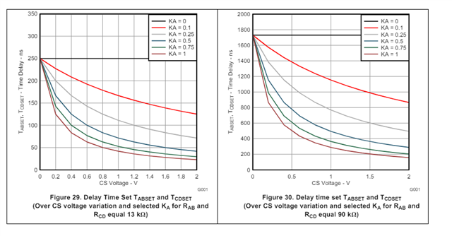
    You might be able to use these characterization curves from the data sheet to try to set the timing.  I have put them below. 

    For one case were you do need as much delay use an RAB of 13 Kohm.  Then adjust the KA ratio for the curve that is closest to what you need.

    For the leg LEG CD you would use 90 kohm and adjust the KA ratio to the curve that is closes to what you need.

    Regards,

    Mike

  • Hi Mike,

    I have already tried using these curves.  Setting RAB = 13k and RCD = 90k does not help since we need the same delay (120ns) for the AB and CD legs at full load, but vastly different delays for those legs at light load, 260ns for AB while need 700ns for CD.

    Regards,

    Nitish

  • Hello,

    The CD leg generally achieves ZVS faster than the AB leg due to the reflected output current providing extra energy to achieve ZVS.

    What you have reported is opposite to what it should be.  Could you double check this? 

    You may be able to decrease the delay times by increasing the size of Ls to help the other leg achieve ZVS faster on the leg that is slower to achieve ZVS.

    Please note that the resonant tank frequency on both switch nodes is the same.  The only thing that is different is the amount of energy to transition the switch node. 

    Regards, 

  • Hi Mike,

    Thank you for your response.  What I have reported for light loads is what we actually see in our system....we have checked this multiple times.

    For that reason, we have had to add switch node capacitance on the AB leg in order to reduce the tank frequency on that leg.

    We don't have the liberty of changing Ls size.

    Given what we are seeing, we can solve our issue by connecting an effective "variable resistor" so to speak, between DELCD to GND, which will appear to the DELCD controller pin like a higher resistance at light loads while lower resistance at full load.

    Can you help provide us with a functional behavior of the DELCD pin with respect to ADEL?  Does it look like a voltage source or a current source?  What is the voltage on it with respect to ADEL voltage?  We are looking to see how to effectively model it so that we can connect a simple circuit between DELCD and GND to achieve the above described "variable resistance".

    Regards,

    Nitish

  • Hello,

    Your inquiry has been received and is under review.

    Regards,

  • Hello,

    Timing equation in the data sheet should show how the delay varies with ADEL, DELCD and DEL AB.  I do understand that it is difficult to set the delay timing due to the different dV/dt at the switch nodes and it is a lot of trial an error.

    I did here one idea that you had that shows promise.  That is to adjust the switch node capacitance to change the tank frequency.  Since this is resonant energy it will not calculate as loss.  You might want to see if you make the switch node behaviors have similar dV/dt then you can use the same timing.

    Regards,

  • Hi Mike,

    Would you mind please addressing my request to provide the functional behavior of the DELCD pin?  Specifically, "is it a voltage source or a current source?  What is the voltage on it with respect to ADEL voltage?".  We are looking to see how to effectively model it.

    Regards,

    Nitish

  • Hello,

    Your inquiry has been received and is under review.

    Regards,

  • Hello,

    I have discuss this with the IC design team and there is not a detailed block diagram that we can share with you.

    However the ADEL and ADELAB/CD pins program an internal current mirror.  The ADEL voltage is passed through an internal buffer to the ADELAB/CD pins.

    With this information you could characterize the turnon delays vs the voltage at the ADELAB/CD pins based on the ADEL voltage.

    Regards,


  • To add more clarity here, you can only sink current from DELCD pin to reduce the "effective" resistance, but not injecting current into the DELCD pin.

    Like Mike suggested, you can measure the DELCD pin voltage and observe the deadtime change to tune your active circuit. 

    I don't recommend to touch ADEL pin since it is linked to other settings.

  • Hello Mike,

    Are you saying that ADEL pin voltage appears at the DELAB, DELCD pins?  Can you or your IC team tell us the current sourcing limit on those pins?

    Regards,

    Nitish

  • Hi Mike / Ning,

    I missed readings Ning's message.

    In relation to my earlier message from a few minutes ago, please also advise if the replica of ADEL pin voltage appears at the DELAB, DELCD pins.  Or, is it shifted by a certain value, or is the average value of the ADEL pin appearing at the DELCD pin?  I can certainly try to measure the DELCD pin voltage, but it will help to get your input too.

    In my earlier message, I used the term "sourcing" capability....while Ning used "sinking".  I meant the current going into the external resistor to ground, which is what Ning meant.

    Regards,

    Nitish

  • Nitish,

    No, ADEL is not connected to DELAB from circuit perspective. You can keep your ADEL setting as is, since it impacts AB leg too. Just focus on DELCD pin setting. It is probably easier to deal with one variable anyway.

    Best,

    Ning

  • Hi Ning,

    I understand that ADEL is not connected to the DELAB / DELCD pins.  Can you please address my specific questions:

    (1) Does a replica of ADEL pin voltage appear at the DELAB, DELCD pins or is it the average value?

    (2) Is the version of ADEL voltage appearing on DELAB or DELCD pins shifted (dc offset) by a certain value?

    Regards,

    Nitish

  • Hi Ning, in addition to the two questions above, please also address the third one below:

    (3) What is the maximum amount of current that the DELCD (or DELAB) pin is rated to safely "sink" to the external resistor to ground connected to it?

    Regards,

    Nitish

  • Nitish,

    Answers to your questions:

    1) no

    2) no

    3) you can measure the DELCD pin voltage while sinking current from it, as long as the effective resistance is > 13kohm, it should be fine. Let's say, the passive resistor is 90kohm, active resistor circuit can give you 7x dynamic range, which is plenty in my opinion.

    Best,

    Ning

  • Hi Ning,

    Thank you.  I will check the voltage on DELCD pin.

    Nitish

  • Hello Ning / Mike,

    I have tried measuring the voltage on DELCD pin.  The node is very sensitive and I have destroyed my converter while trying to measure the average value of voltage using a high input impedance voltmeter (10Mohm).  Before the unit blew up, I managed to get some readings, but they were jumping all over the place.

    Does the DELCD pin function care about the average current going out of that pin into the external resistor or does it care about the peak value of current waveform at that pin?

    Sincerely,

    Nitish Agrawal

  • Hello,

    DELCD and DELAB should track the ADEL pin.  I am not sure why putting a volt meter across it would cause it to blow up.  Or even why putting 10 kohm in parallel would be an issue.  However, if you have something coupling into the voltmeter cables injects a signal on these pins it cause an issue.

    If you want to evaluate these pins try using scope probes and have the scope grounds as close to the UCC28950 ground as you can get it.  Also make sure the scope probe wires don't cross anything that could pick EMI.  Putting your scope probe across the transformer could do this or even being in parallel with high current paths in your design.

    Regards,

  • Hi Mike,

    Does the DELCD pin function care about the average current going out of that pin into the external resistor or does it care about the peak value of current waveform at that pin?

    Regards,

    Nitish

  • Nitish,

    Please give us few days to get back to you.

    In the meantime, we don't recommend to physically place the multimeter probe on the IC pin as risk of accidental shorting to adjacent pins is high. It is always recommended to use oscilloscope to measure the signal, especially during switching.

    Thanks,

    Ning

  • Hello,

    The ADEL pin is set based on the peak voltage and not the average.

    Regards,

  • Hello Mike,

    My question was not about the ADEL pin.  Can you please address whether the DELCD pin function care about the average current going out of that pin into the external resistor or does it care about the peak value of current waveform at that pin?

    Regards,

    Nitish Agrawal

  • Hello,

    Your inquiry is under review and I will get back to you shortly.

    Regards,

  • Hello,

    The timing is set based on the current coming out of the DELCD pin when the duty cycle is terminated.

    This occurs every switching cycle.

    Regards,

  • Hi Mike,

    Thank you for your response.  From your reply, I understand that the value of current coming out of DELCD pin at the time when the duty cycle is terminated is usedslum277a_ADEL_tied_to_CS.TSC to set the deadtime.

    I ran the TINA-TI simulation file slum277a.tsc after connecting the ADEL pin to the CS pin.  It shows a DC value of voltage present on the DELCD pin (with ADEL tied to CS).  It appears that the simulation result is incorrect.  Can you confirm?

    Regards,

    Nitish

  • Hello,

    Your inquiry is under review and I will get back to you shortly.

    Regards,