Other Parts Discussed in Thread: UCC39002, , UCC29002
Hi.
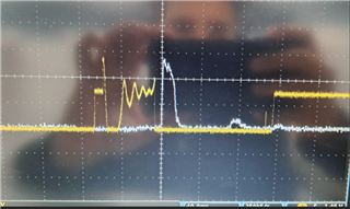
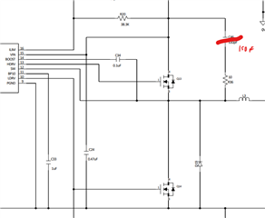
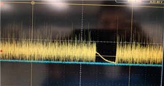
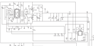
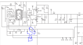
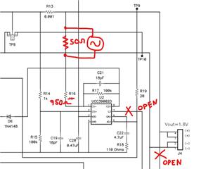
We are using two TPS40054 chips to get 5.1V and 3.3V outputs, a UCC39002 for load sharing control, and a hot-swap controller for reverse current protection. Our design was working fine, but we had to replace the High- and Low-side FETs in the Buck converter from FDB13AN06A to IRF1018ES. We also replaced the UCC39002 surface-mount with a UCC29002 through-hole. The ratio between Qgs/Qgd is better in the Infineon MOSFETs than the Onsemi ones; however, we are encountering issues with the new MOSFETs. When we connect the load-sharing controller to the circuit, hot swap controller enters in fault mode. However, when we replace the new MOSFETs with the old ones, the problem seems to be resolved.
Additionally, the issue only occurs under no-load or light-load conditions; when we connect a certain load to the output, the power supply starts working again.
Do you have any information on how the MOSFETs and the load-sharing controller might be related in this context?
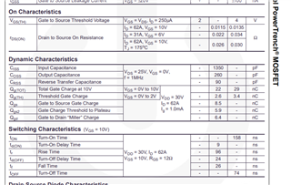
Infineon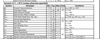
OnSemi