This thread has been locked.

If you have a related question, please click the "Ask a related question" button in the top right corner. The newly created question will be automatically linked to this question.

TPS92520-Q1: An LED open circuit fault CASE3

Part Number: TPS92520-Q1


hello,expert

I have checked the specification sheet of TPS92520 and have some questions about output open circuit fault case 3:

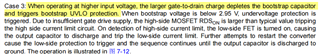
We can see the description in its datasheet,but i have some  questions,please help explain in details.

1) When operating at higher input voltage, the larger gate-to-drain charge depletes the bootstrap capacitor and triggers bootstrap UVLO protection?what is the "larger gate-to-drain charge" ?  

2) What caused the bootstrap capacitor undervoltage protection? Is it due to an open load?

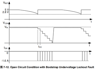
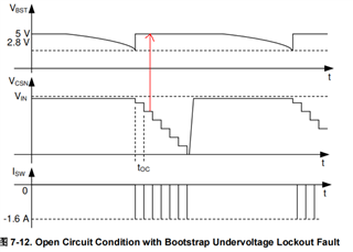
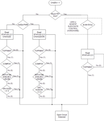
My understanding: First, the load is open → the chip operates in the minimum off time mode→Causing insufficient conduction time of LS MOS→bootstrap UVLO →HS LIMT→LS  LIMT →repeat LS  LIMT

Is my understanding above correct? Is the order correct?

3)When a low side MOS LIMT event occurs, will LS mos also immediately shut down? 

4)What situations would trigger bootstrap UVLO protection if it were not for an open load condition? 

5)if i apply the PWM DIMMING, Will bootstrap UVLO protection be triggered during PWM OFF time? 

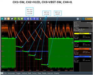
I have also seen other similar posts on the forum, but I did not understand them. Please help me explain them in detail again

thank you

best regards 

  • Hello Qinlei,

    1)  That is due to FET inside our part.

    2)  When you hit either HS ILIM or LS ILIM you are turned off for the duration of tOC (over current retry time).  That time is enough to have the bootstrap capacitor to be discharged below the BSTUV threshold of the device and the LS FET has to be turned on prior to retrying, but it trips the BST UV fault and sets the bit.  

    3)  Yes, once LS ILIM even occurs both LS and HS FETs are turned off and the COMP capacitor is discharged so that the next time it tries to turn on it does a soft start.  

    4)  What do you mean by UVLO?  Are you talking about the external resistor divider on the UDIM pin??? or do you mean the BST UV which is a kind of UVLO for turning on the HS FET?  I am assuming that is what you mean. BST UV is triggered if you don't have a large enough boot strap capacitor such that the voltage on the bootstrap capacitor is above the BSTUV threshold.  The longer the off time of the PWM the lower the voltage drops across the bootstrap capacitor due to leakage.  I generally tell people to oversize the bootstrap capacitor to avoid having BST UV being triggered.  Case 3 Open Circuit happens because of ILIM event.  Once this happens, you have a Toc for a pretty long time and you also have a forced softstart which actually causes the LS FET to be turned on for a really long time.  In an open circuit the output voltage goes to almost the input voltage, When the output capacitance is large the bootstrap capacitor is discharged alot, and there is a soft start where the LS FET is turned on for a long time during the soft start.  That means the LS FET sees the current to charge the bootstrap capacitor while at the same time it discharged the output.  If the current to do that is too large it hits the LS ILIM.  

    6)  That depends on the capacitance used and the condition.  If the off time is too long and the capacitor is too small then you will trigger the BST UV condition and that will set the BSTUV bit and it will force the LS FET to turn on to recharge the bootstrap capacitor before turning on the HS FET and starting up normally.    

    Use this algorithm to detect and open circuit:

  • hello,expert

    thank  you for your reply , i have another question about the CBST,

    It is described in the specification as follows:

    1) the IQ(BST) is the Leakage currents During PWM OFF ,right  ? 

    2) According to the formula ,C=Q/U ,I=Qt   ,As far as I understand, does the formula need to add red parts?

    Or we don't need to calculate in such detail, just rough calculations? 

    /resized-image/__size/320x240/__key/communityserver-discussions-components-files/196/pastedimage1715302832044v1.png

    thank you

    best regards 

  • 1/fPWM is the period TPWM of the PWM cycle so that is the worst case off time.  

    This equation only accounts for the leakage from BST pin to SW, there is another path that isn't included in the datasheet because we can't measure it.  That leakage path is from BST to GND, inside the part.  If you use the table you should be fine.  

    -fhoude

  • hello expert

    i would like to ask Is there BST UV at the position of the red arrow?

    1)I have reviewed your previous question answer records,From the figure below, it can be seen that LS limt occurred simultaneously with BST UV,

    But from the above figure, it can be seen that the BST voltage at this time is normal at 5V,Which one is correct?

    2) I'm sorry that I didn't understand the process of determining the open circuit. Could you please describe the process in simple language?

  • 1)  The diagram isn't correct, trust the waveforms.

    2)  Just follow the flow diagram.  What don't you understand?  Be specific.  

    -fhoude